 CONGRATULATIONS. All the carefully constructed hardware and software curriculum you have explored over the past years have positioned you for the next-to-deepest level of MCU software over our final four weeks (the deepest level being machine language, but we're not completely insane). Optimization, efficiency and, ultimately, productivity, are some of the noblest goals the embedded engineer sets out to realize and assembly language enhances those targets. Your superior communication skills (text and video) are simply the icing on the cake.
What is somewhat unique about our ACES program is that much of the curriculum we explore is based on tools developed within the DES by those students that have left their talents as gifts for us to benefit from, the latest of which as you are about to realize in the DDP. To underscore the significance of this you are encouraged to read the history of this particular platform and the history of our program and philosophy, in general.
DDP Task Sequence
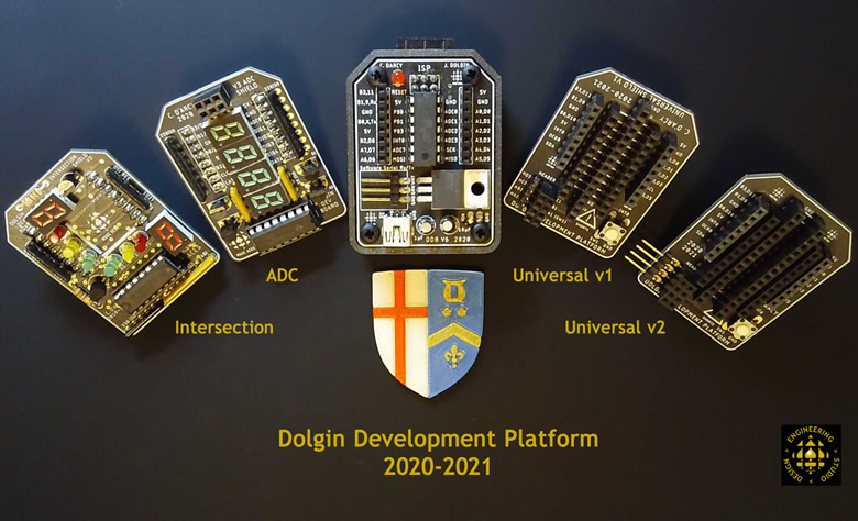
 DDP is an acronym for the Dolgin Development Platform. This hardware technology platform has evolved since its inception in the 2019/2020 ICS4U year to encompass the Dolgin Development Board motherboard (DDB), together with an array of daughterboards (ADC Shield, Intersection Shield and Universal 1 and 2 Shields). What appears below is a carefully-considered sequence of tasks for our remaining two months.
Throughout this session you will find supporting assets on  Dolgin Development Platform.
0. DDBv7 Hardware Assembly
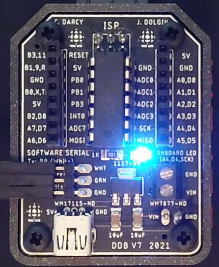
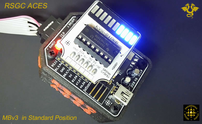
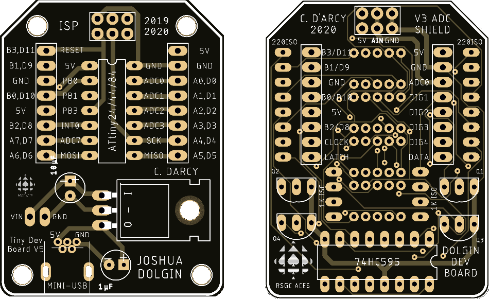
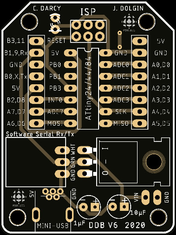
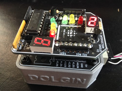
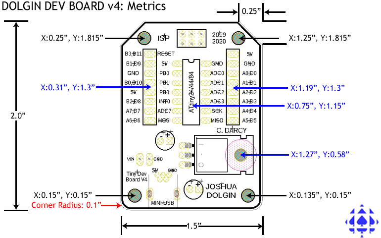
 Your first (pleasant) task will better acquaint you with the DDBv7 hardware platform. From the Parts Table below you can see the time and space-saving benefits of the pre-assembled SMT parts by JLCPCB (5V regulation and onboard LED/resistor pair). The remaining THT components will be provided to you for completing the assembly of your Dolgin Development Board Version 7 (DDBv7). In our first class of Block 4 (March 29) we'll go over specific soldering tips and reminders for the DDBv7. Be sure to listen carefully as replacement parts are obviously difficult to address under current conditions. Please arrive to class on Wednesday March 30 with your device ready for duty.
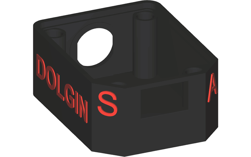
J. Vretenar (ACES '21, Carleton '25) is deserving of special mention for supplying the 3D printed cases for the DDBv7 based on J. Dolgin's design. Having said that, 21/22 ACES Liam and Harrison are working to get the MMU Prusa back up to speed to print another set of DDP cases. We'll keep our fingers crossed their effort bear fruit. @22/3 ACE Seb Appleyard has tweaked the design and will provide a case for everyone. Here is a photo of how the Schurter power jack intergrates into the platform. My only suggestion would be to mount an underside terminal block for easier connect/disconnect.
1. DDBv7: IDE Installation
 The oft-maligned Arduino IDE has served us well to this point. Indeed, it could even support and sustain our AVR Assembly Language ambitions over our final stretch, however, the experience gained by moving to a more comprehensive development environment and tools provides a richer exposure and positions you well for the even more comprehensive IDEs your futures will introduce.
The most appropriate IDE for ACES programming of the AVR-8 (AVR-C & Assembly) is the one provided by its creator, ATMEL, called ATMEL Studio v7. ATMEL was purchased by Microchip a few years back and although the latter promotes its own IDE, Microchip Studio Lab X, the application is not stable enough for our purposes. Both applications are Windows-based development environments that need to be installed on your Mac laptop. Here are the steps required (2023) to get a working AS7 instlltion on your laptops,
- Install Windows 10 on your Mac with Boot Camp Assistant
- Install Atmel Studio 7 on Windows
- Install the Arduino v1.8.19 (Legacy) IDE (for ARVDUDE)
- Install the Windows USBTiny Driver from Adafruit
2. DDBv7: In-System Programming
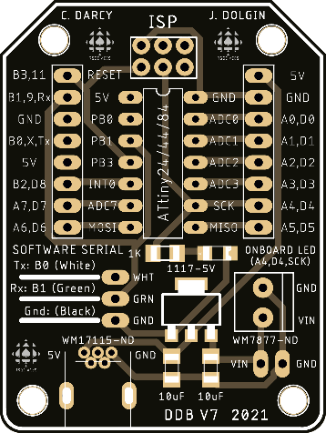
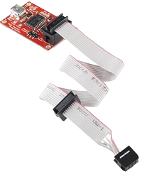 With your DDBv7 physically assembled, we are now ready to begin exploiting its capabilities. Whereas the Arduino platform has onboard USB to Serial support, our leaner DDBv7 relies on ISP programming. For this, you'll use your trusted Sparkfun AVR Pocket Programmer, inserting the ISP cable into the undermounted 2×3 Shrouded ISP Header (Wurth) connector. Whereas this is a familiar and efficient means to reprogram our AVR MCUs, it does come with a significant downside as the SCK, MISO, and MOSI (PORTA4:6) pins are required to perform the reflashing.
Another design feature of the DDBv7 is that once your project is functioning, you can remove the ISP connection, detach the programmer and simply insert its power cable into the USB MINI B Connector (Molex) connector on top to power your prototype. Very convenient (it's likely clear to you by now that the DDBv7's access point design decisions that you've encountered already were purposely intended to maintain low headroom on the top of the platform. Hence, you'll have unobstructed access to the ATtiny84's header pins).
A third power solution is the use of the undermounted 2.1 mm Power Jack (Schurter). The JLCPCB-assembled OT-223 LM1117 Voltage Regulator (C277893) yields the 5V supply your ATtiny84 requires. This strategy offers the best solution for maximum power as it is not restricted to the ~400 mA current limitations associated with your computers' USB ports. Furthermore, the DDBv7's onboard screw terminal block facilitate access to the voltage In (VIN) allowing both control and drive supply levels to function in tandem.
Task.
 We need to confirm we can upload code from MS/AS7 to the DDP with your Sparkfun Pocket Programmer. This requires a one-time configuration.
- Watch this video:
 Using a USBtiny Programmer with Atmel Studio
- Here's the web tutorial of the video: http://www.crash-bang.com/using-usbtiny-with-atmelstudio/
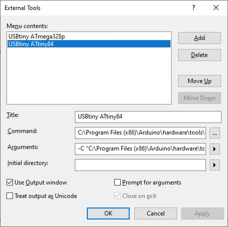
- Under the Tools Menu, select External Tools... and build a USBtiny ATtiny84 tool that will create a script to convert and upload our assembly source file to the ATtiny84 target on the DDP. Click the image to the right to enlarge. On my Windows version I have,
Title: USBtiny ATtiny84
Command: C:\Program Files (x86)\Arduino\hardware\tools\avr\bin\avrdude.exe
Arguments: -C "C:\Program Files (x86)\Arduino\hardware\tools\avr\etc\avrdude.conf" -c usbtiny -p t84 -v -v -v -U flash:w:$(TargetDir)$(TargetName).hex:i
2*. DDBv7: Programming and Debugging with ATMEL-ICE
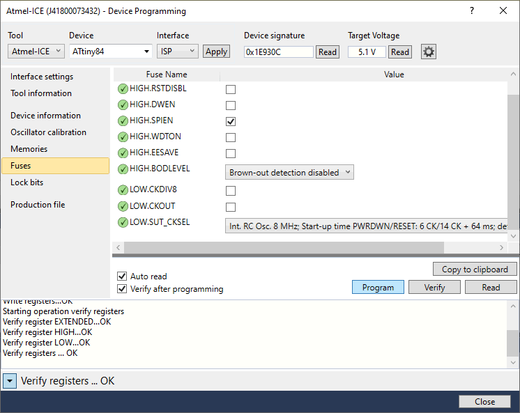 Before proceeding, I would be remiss if I did not acknowledge an alternative to In-System Programming (ISP) with the SPP. Microchip offers the ATMEL-ICE programmer/debugger that provides some advantages over the SPP. Once cabled, the ability to examine and set the fuses, flash Program as well as EEPROM memories, and to do so for the DDBv7, UNO, Nano and most other AVR Dev boards are compelling reasons to consider this device for embedded development. The graphic to the right displays one view of the Device Programming dialog box enabled through the use of the ATMEL-ICE-BASIC.
On the other hand , the numerous shortcomings of this strategy, the cost being but one, are sufficient for me to withhold recommendation at this time. I'll let this site introduce you to some of them. https://www.bigmessowires.com/2018/06/13/atmel-ice-wiring-horror/
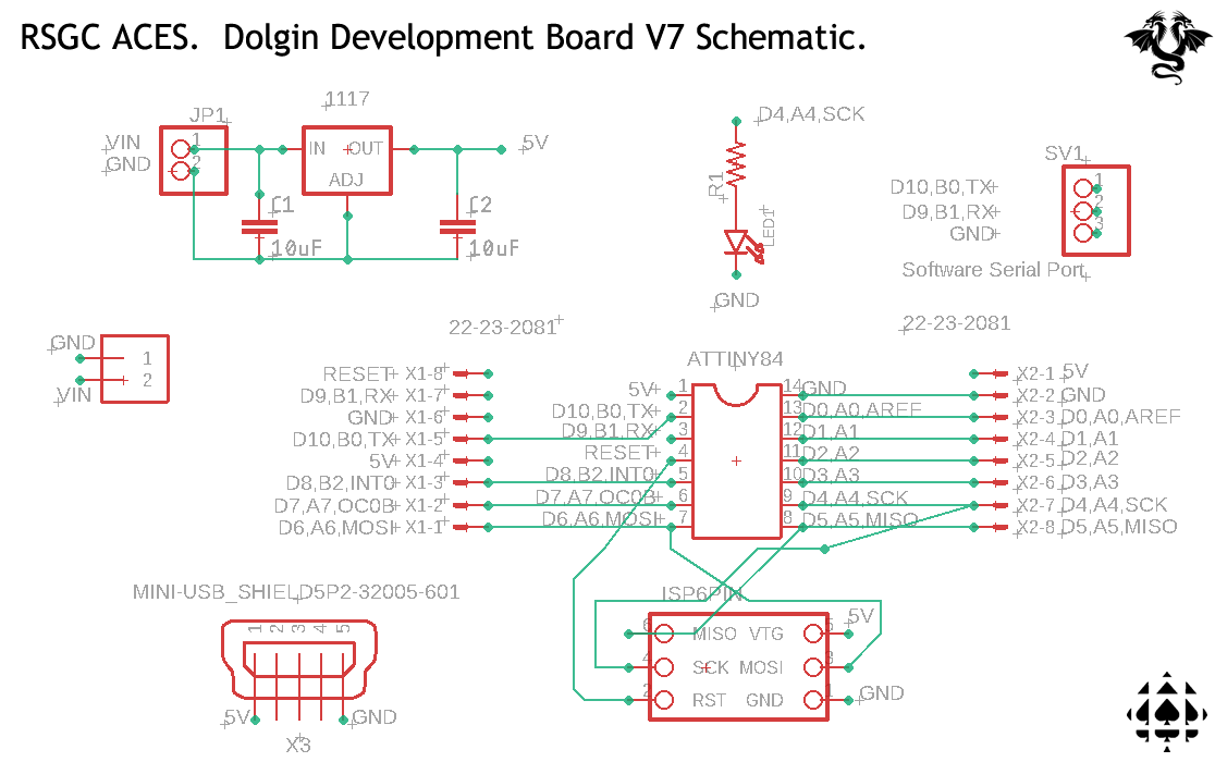
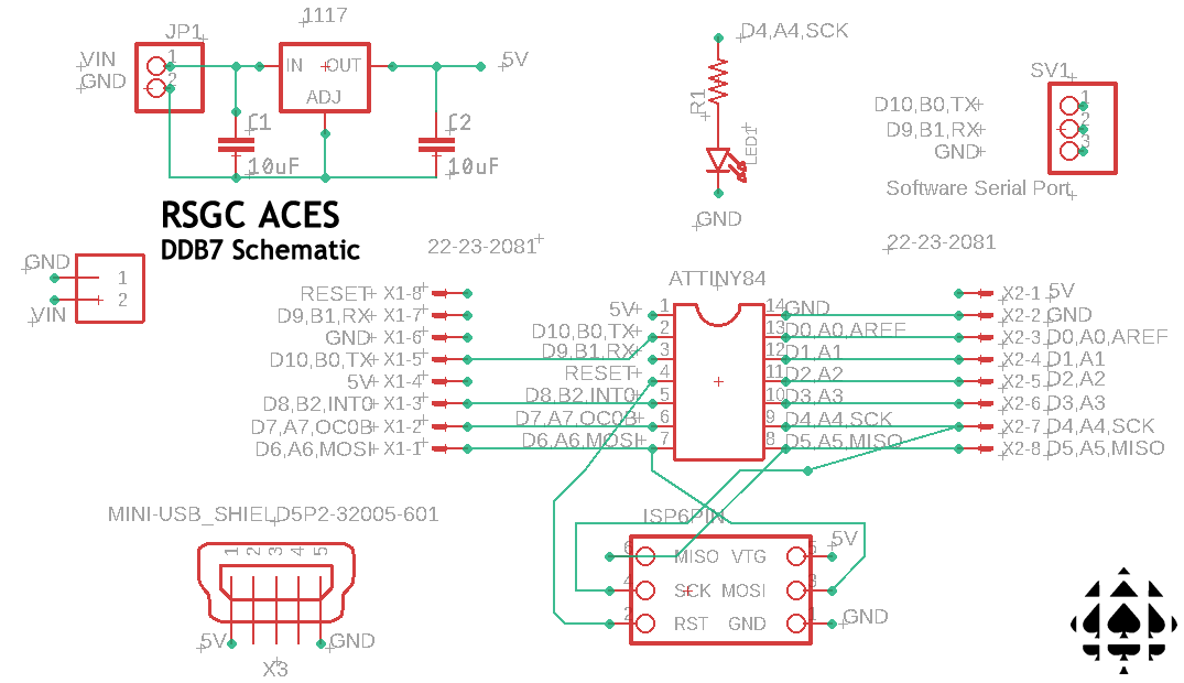
3. DDBv7: The Schematic.
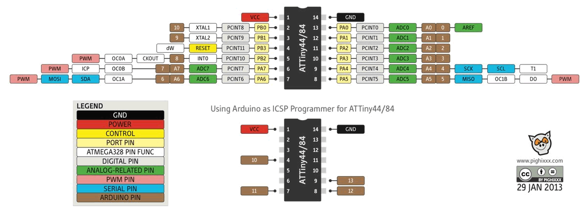
You are encouraged to review the schematic below ro familiarize yourself with the mapping of the ATtiny84 and its supporting resources. Click to enlarge.
4. DDBv7: The OnBoard LED
Following the tradition of Arduino Dev boards, the DDBv7 was designed with an onboard (blue 1206) LED tied to digital pin 4 (PORTA.4). Can you think of a reason why this pin was chosen? For your first series of DDBv7 Assembly programs you are asked to put this LED through its register-level coding paces.
Task.
 Click on the images to the right and below to familiarize yourself with how the DDBv7 breaks out the ATtiny84's pin arrangement and supply (5V and Gnd) options.
- Using Finder, create a folder to store your AVR Assembly Language projects.
- Launch MS/AS7
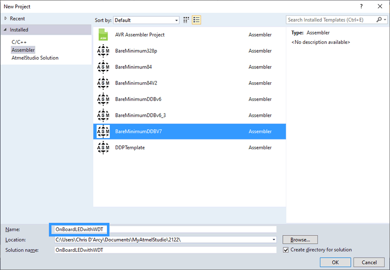
- Select File>New>Project
- Select Assembler | AVR Assembler Project and complete the dialog box using OnBoardLED as the Project's name and browsing to the folder created in Step 1 as the Location
- In the Device Selection dialog, choose ATtiny84 and continue
- The project is now created with the driver file entitled, main.asm.
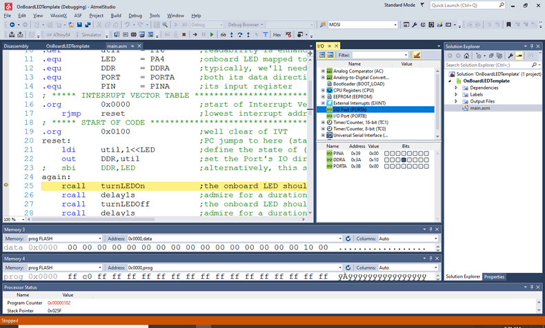 Close the project and replace the default main.asm with this main.asm
- Reopen the project and review the working file, awaiting further execution instructions.
- Modify the sketch to confirm you can blink an LED on any of the other digital pins. You might wish to develop alternate flashing of the 3 or 5 mm bicolor LEDs.
- For those motivated ACES I encourage you to improve your AVR Assembly Language skills by returning to the Schaffer Traffic Light of early Grade 11. Insert your STL into your DDB7 and code up a working program using this task's code as a starting point.
5. DDBv7: Project Template
 Just as we did in early Grade 11 to create an efficient base template for code development within the Arduino IDE (modification of BareMinimum.ino), we will create also basic template for AVR-8 Assembly Language coding in Atmel Studio 7. You'll also find this code on our Dolgin Development Platform. The code contains far more more than we need right now, but this language can be tricky at the start so better to remove what's not needed than struggle to recall what's missing.
;PROJECT    :Template23
;PURPOSE    :Code shell for AVR-8 AVR Assembly projects for the DDP (ATtiny84)
;AUTHOR     :Your name
;DATE       :2023 04 14
;DEVICE     :Dolgin Development Platform. Version 7.
;MCU        :ATtiny84
;COURSE     :ICS4U
;STATUS     :Not Working (Yet)
;REFERENCE  :http://darcy.rsgc.on.ca/ACES/Datasheets/ATtiny84.pdf
;NOTES      :
;.include   "prescalars84.inc"  ;assembly directive equivalent to compiler directive #include
.def        util    = r16       ;readability is enhanced through 'use' aliases for GP Registers
.equ        DDR     = DDRA      ;typically, we'll need the use of PortA
.equ        PORT    = PORTA     ;both its data direction register and output register and, eventually,
.equ        PIN     = PINA      ;its input register
; DATA Segment declarations
.dseg                           ;locate for Data Segment (SRAM) requirements (default start at 0x0060)
var:        .BYTE 1             ;reserve one byte for a variable (the label is the symbol)
; CODE Segment (default)
.cseg                           ;locate for Code Segment (FLASH)
; ***** INTERRUPT VECTOR TABLE ***********************************************
.org        0x0000              ;start of Interrupt Vector Table (IVT) aka. Jump Table
    rjmp    reset               ;lowest interrupt address == highest priority!
.org        EXT_INT0addr        ;External Interrupt Request 0 (prefined in tn84def.inc)
;   rjmp    INT0_vect
;.org		INT_VECTORS_SIZE	;locate flash data requests here
ArrayStart:						;label is the address/name of the array
.db		21,22					;populate the array with (single) bytes
.dw		2122					;populate the array with words (two bytes)
ArrayEnd:						;label marks the end address of the array
; ***** START OF CODE ********************************************************
.org        0x0100              ;well clear of IVT & program memory data
reset:                          ;PC jumps to here (start of code) on reset interrupt...
	ldi		util,low(RAMEND)	;AS7 appears to do this by default
	out		SPL,util			;however it is wise to ensure the SP
	ldi		util,high(RAMEND)	;starts out at the highest SRAM address
	out		SPH,util			;
	ldi		XL,low(ArrayStart<<1)		;position X to start of array
	ldi		XH,high(ArrayStart<<1)	;
	ldi		YL,low(ArrayEnd<<1)		;position Y to end of array
	ldi		YL,high(ArrayEnd<<1)		;
	movw	Z,X					;position Z (index) to start of array

wait:
    ldi     util,0xAA
    sts     var,util
    rjmp    wait                ;repeat or hold...
Activity: Project Template Creation in 2 Steps
Step 1. First, we need to create and explore an assembly code shell that will serve a role similar to the BareMinimum sketch we used repeatedly in the Arduino IDE.
 Open MS/AS7 and create a New > AVR Assembly Project in your DDP
 Assembly folder with the name Template84.- Within the Device Selection dialog, select ATtiny84.
- Use the code above to replace the default
main.asm code supplied and listen carefully as we review it. Make sure it builds without issue. Edit, if necessary.
- Under the Project menu, select the Template84 Properties option and select the Tools button. Select Simulator as the debugger/programmer.
- Select the main.asm tab, launch the Debug menu and select, Start Debugging and Break.
- Now, simply marvel at what comes next...:)
- Within the Solution Explorer panel to the right, select the Dependencies folder and double click the
tn84def.inc file to review the complete list of .equates available to your assembly code. You are encouraged to maximize their use.
 Step 2. Finally, MS/AS7 provides a seamless method for creating new projects from an existing code shell.
- After saving
main.asm, select Export Template... under the File menu.
- Select Project Template and then complete the fields in the subsequent dialog box, entering
BareMinimumDDBV7 as the Template Name.
- Feel free to use the ACES ASM graphic at the top of this task for your Icon Image, and select Finish when complete.
- With luck, the next project you create can be based on your
BareMinimumDDBV7 template, providing a more productive use of your time and effort.
 6. DDBv7: Schaffer Traffic Light: Introduction to Assembly Language I/O Port Manipulation
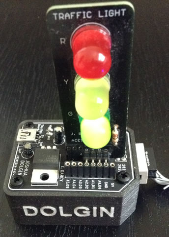
A year before his famed Rubik's Cubic Solver ISP in Grade 12, J. Schaffer created this handy legacy device for future ACES to practice their high and low level port manipulation skills.
Task
- Insert your Schaffer Traffic Light into PORTA pins 0 through 2 as shown so the ground pin of the STL conveniently inserts into the GND pin of the DDB.
- Use your new Code Template to create a project called SchafferTrafficLight.
- Develop AVR-8 Assemlby Code that will continuously cycle through the LEDs (G → Y → R → G → ...) with Green and Red remaining on for 3 s each and Yellow, but 1 s.
- Delete any unnecessary code.
- Comment EVERY other remaining statement, effectively. This is important.
7. DDBv7: Schaffer Traffic Light with WDT Interrupt

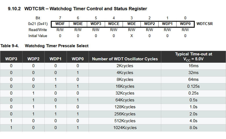
 As convenient as the Mulvey/Morland utility is, simply wasting clock cycles in a loop is not the most productive strategy for embedded software. We should engineer better. The groundwork for an improved STL sequence code was laid in the previous months when you undertook a register-level exploration of the Watchdog Timer interrupt on the ATmega328P. The beauty of ATMEL family of MCUs is that not much changes in terms of Register design between mega- and tiny- families as you will discover in the ATtiny84 Datasheet's Register Description of the Watchdog Timer Interrupt.
Task.
 Open last week's AS7 Assembly project, STLwithWDTInterrupt.atsln that we had just started.
- Open the Windows File Explorer, navigate to your main AVR Assembly Project Folder, and create a new directory folder called include. This is where you can store and reference all your future AVR Assembly .include files.
- Download the include file, prescalers84.inc, into your new include directory/folder.
- Go back to Atmel Studio and open Project> SchafferTrafficLightwithWDT Properties... > Toolchain > General > Include PAths and add the path to your new include directory/folder.
- At the start of your program, configure the Stack Pointer as dicsussed.
- Similar to your Arduino/Processing experience, create a function called setup that will undertake some one-time initializations. call your setup function immediately after your SP initialization.
- Within setup configure the WDT to interrupt (only) every 2 s.
- Implement an WDT Interrupt ISR that advances the STL light
- Comment your code thoroughly.
8. DDBv7: shiftOut: Morland Bargraph
 With assembly level port manipulation skills underway we can turn to a familiar friend to strengthen our command of these skills in the efficient manipulation of bits to emulate the shiftOut
() function.
Design Considerations. In designing the MBv3's minimal 6-pin breakout board there simply was no optimum arrangement that enabled it to be a UNO-compatible appliance. Wherever it is placed it puts an unacceptable strain on the port pin forced to serve as the 5V source. So, given the MBv3's versatility in so many ACES' projects, the ATtiny84's pin breakout strategy accommodated an optimal position for the MBv3 on the DDBv7. Click the image to the right to enlarge. The 5V and GND supply pins are positioned correctly to provide the appliance with full power access. The only issue that remained was the non-critical conflict with the onboard LED. This has been addressed in the DDBv7 with its relocation to Pin 4 (PA4/SCK).
Task.
- Using your AVR Assembly DDBv7 tempate as a base, create an AS7 Assembly project, entitled MBv3Counting.atsln.
- The objective of this project is to present continuous binary counting on your MBv3, starting a 0 with rollover after 255.
- Incorporate the Watchdog Timer Interrupt to control the pace of counting. 0.125 s works well.
- Optimize the assembly code as much as possble and document your code THOROUGHLY (every instruction requires a compact, meaningful comment)
- Place your Assembly code (Courier New, 9 pt) in a background-shaded table just as you have with high-level code with a Code section. After insertion, be sure to align the comment semicolons. Presentation accounts for a great deal in my marking priorties (it goes a long way to convince me you care :).
8. DDBv7: Memory Considerations
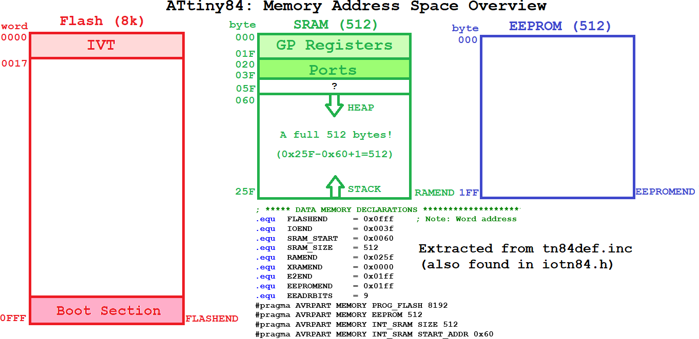 Familiarity with the AVR's three memories (Program Flash, SRAM and EEPROM), together with the dedicated reserved addresses within Flash and SRAM are essential for embedded systems optimization.
Program Flash reserves the first set of addresses for its Interrupt Vector Table (IVT). These addresses are populated with jmp instructions to Interrupt Service Routines (ISRs) as required and are specific to each MCU.
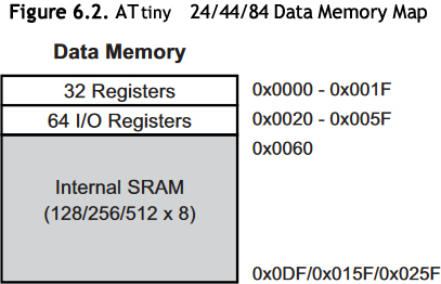
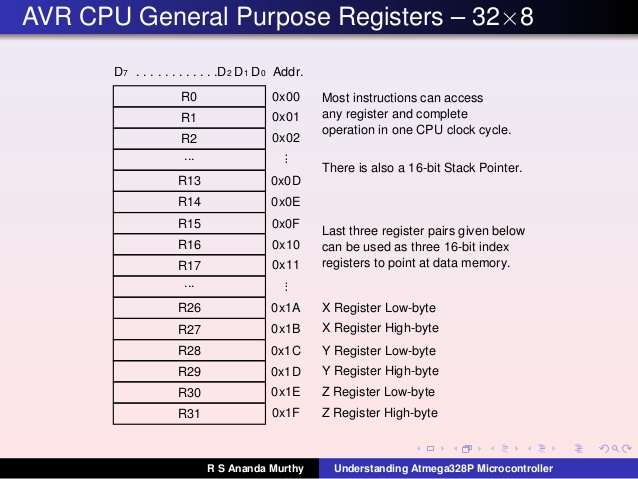
AVR SRAM reserves and organizes the first set of addresses into distinct areas for various purposes including RISC instruction support. The first block, addresses 0x0000 to 0x001F, are the 32 instruction registers named r0 through r31. The second block on the ATtiny84, addresses 0x0020 to 0x003F, are for both the IO Ports and peripheral-specific (Timers, ADC, etc.) register configuration and support. The highest address in this second block, 0x003F, is the critical Status Register (SREG).
The balance of SRAM is used for your code's memory requirements with the Heap growing upwards from 0x0040 andthe System Stack growing downward from address 0x025F. We will have more to say about these concepts as time permits.
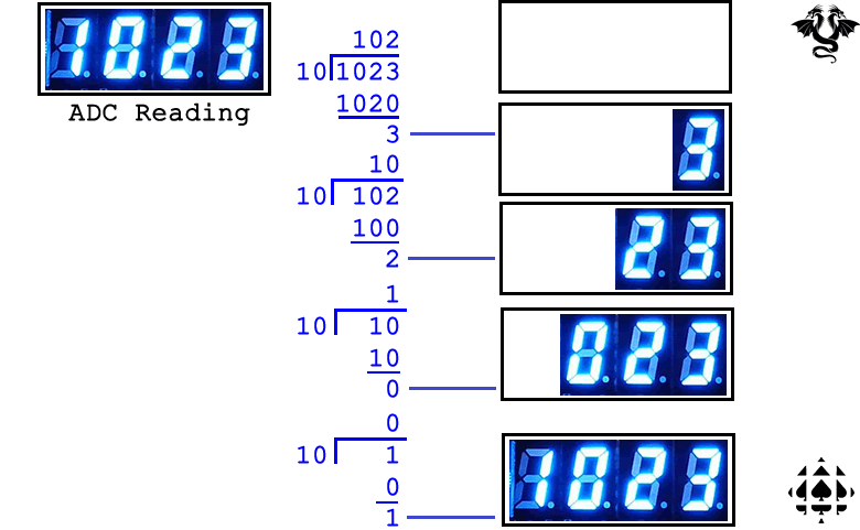
10. DDBv7: Indirect Addressing (Pointers): Array Processing
10. DDBv7: DDP: ADC Shield
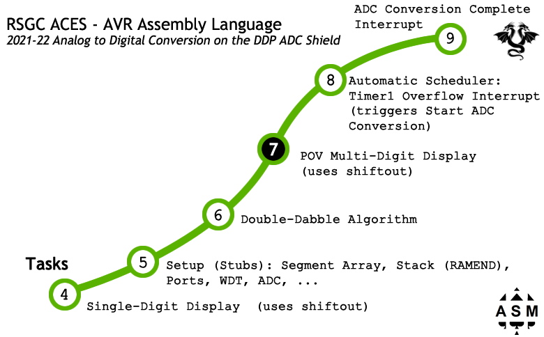
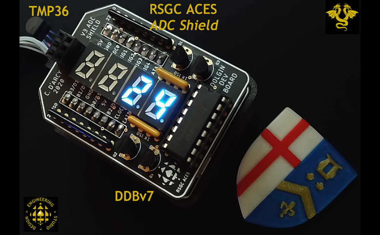
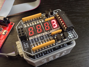
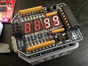
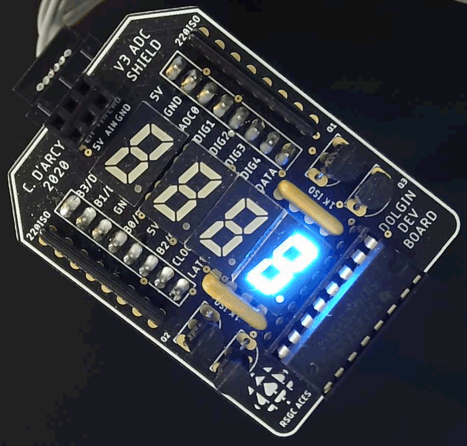 Familiarity with the AVR Assembly Language shiftOut sequence on the Morland Bargraph opens the door to the DDP's ADC Shield. The ADC Shield is designed to present input from the 10-bit Analog-to-Digital Conversion feature of the ATtiny84 (oddly enough, the DIP14 ATtiny84 offers 8 separate ADC channels as compared to the DIP28 ATmega328P's 6) with 4-digit seven segment display output. The full implementation of the device ultimately requires revisiting Grade 10 hardware, Grade 11 PoV software skills together with Grade 12 WDT scheduling and careful register-level port manipulation (among others things :). This week-long investigation is organized into four development stages.
Task.
- Create the MS7 project, ADCShield.
- SINGLE-Digit Display (Shiftout). There are many ways we could begin this project but, for this year, we'll start with continunous cycling through the 7-Segment Lookup Table (LUT) on a single display unit, to familiarize you with array addressing using the X, Y, and Z pointers. Define a 10-element array of segment maps for the 7-segment display in the order ABCDEFGx
 MULTI-Digit Display (PoV). In this stage you will adapt your PoV skills to confirm that, eventually, once the analog reading has been captured in the final phase of this task, your code will readily present it.
- Later this week we'll learn how to convert the two-byte (10-bit) output of the MCU's ADC unit into the four separate BCD digits required for presentation on our discrete displays. Until then, we'll hard-code the four sample digits. Using the .db directive, define the values 1, 0, 2, and 3.
- Implement a flexible, modular, register-level PoV algorithm that balances brightness with minimal flicker using the pseudocode structure as a guide.
- Update your display using your shiftout()skills
- Your code should suppress leading zeroes.
- Comment with conviction.
- Interval Sensing, ADC, and Reporting. In this initial stage, we revisit WDT scheduling with interval Sleep capabilities in developing code that periodically acquires and plots temperature readings from the TMP36 between intervals of sleep. with it is obvious that on the WDT interrupt, our application could accomplish some useful before retiring to sleep again.
-
 Familiarize yourself with the TMP36 in a more 'informative' environment. Review Adafruit's TMP36 terrific tutorial.
- Insert your TMP36 into GND-PA0-PA1
- Save your previous WDTwithSleep project as WDTwithSleepADC.
- Adapt the earlier sketch to have a reading taken of the TMP36 scheduled on a WDT interrupt (every 1s)
- Convert the raw reading to a result in °C and send to the serialmonitor and plotter plotter through the DDB's SoftwareSerial support facility.
- In a future segment, we'll explore the use of register level access to the ADC Conversion Complete Interrupt (IVT #14).
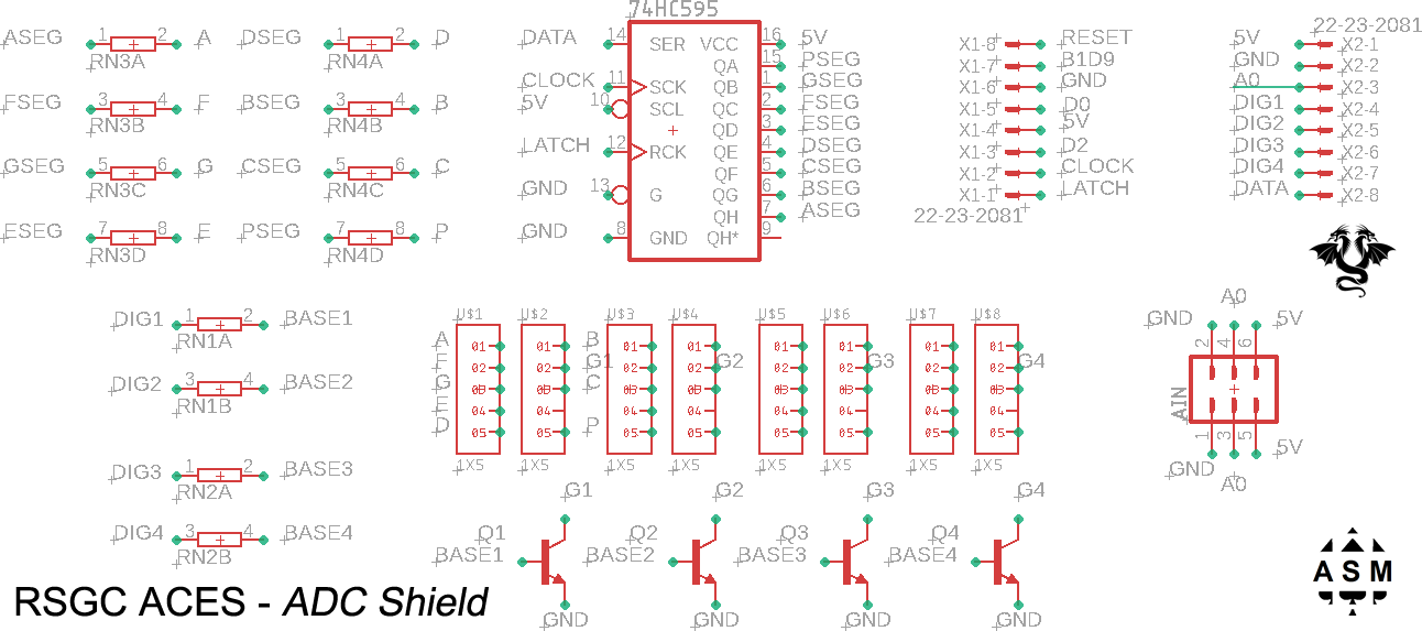 Download the EAGLE Files for this Shield and examine them closely. You'll likely exploit these later in the term when you design your own DDP Legacy Shield.
- Q. How are the signals for the 2×3 female input header arranged?
- Q. Considering the other shield components what software technique is employed to present the reading?
- The displays are small, obsolete 7-Segment displays: (2mm pitch, LA-301VL).
- Q. Which pins have been assigned to base pins of the transistors to sink the respective displays?
- Review the side-by-side pairing of the DDP base (left) and the ADC Shield below (click to enlarge). The silk-screening will enable you to determine and
#define the corresponding port/pin usage. Note. When you create your own DDP Legacy Shield do not overlook the benefits of smart silk-screening to those that follow you.
 Putting it all together. In this final phase we add the scheduling of ADC sampling with Watchdog Timer interrupts. A trimpot as voltage divider offers quick response for testing your code. Once complete replace the trimpot with your TMP36. A voltage divider made from an LDR and fixed resistor also creates an interesting experiment while waving your hand over its top.
- Add WDT interrupt support to trigger every half-second, for now.
- Create a history array of preferred length (16-32?) to provide a data smoothing facility. Add a function that will accept a new reading and produce an adjusted average.
- Using the register-level introduction to ADC presented in class, adapt you project's code to trigger the start of conversion on every WDT interrupt.
- On the completion of the ADC, obtain the 10 bit reading from the ADC_Complete ISR and add it to your smoothing average.
- Consideration must be given to the different clocks and prescalers (WDT and ADC) to avoid collisions.
- Convert the average of raw readings to a result in °C using your formula from Part 1. Adjust for the context of the DDP.
- Update your display with the new average.
- Start a new conversion.
- Congratulations. You have achieved another project of lasting significance.
11. DDBv7: Arrays and Indirect Addressing (CharlieStick)
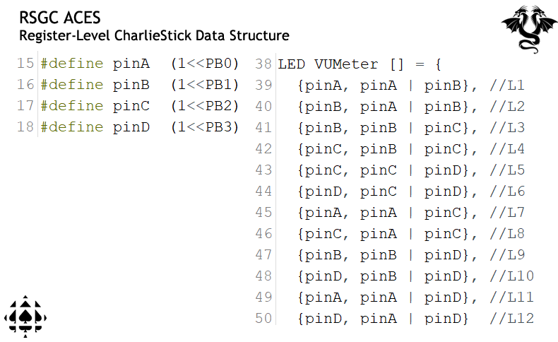 Arrays are an indispensable software data structure that needs to be ported to an AVR Assembly Language context. For this investigation we'll return to the ACES' Charliestick to gain familiarity. In a previous register-level coding task you developed both a DOT and BAR display views. The relative complexity of arrangement of LEDs was simplified through the use of array of structs providing indexed access to the PORT data.
Task.
- Using your freshly-minted BareMinimumDDBv7 Template as a base, create a new project entitled CharlieStick.
12. DDBv7: The Intersection Shield
For this shield experience the Schaffer Traffic Light (STL) gets a significant upgrade in the form of 2-way Intersection simulation with countdown displays in both directions. The device can be thought of a Finite State Machine (of the Moore variety) in which the state transitions are to be triggered through WDT Interrupts you were acquainted with from a previous section.
- Watch this clip of the simulation, DDP: Intersection Shield (1:08)
- Download the EAGLE Files for this Shield and review the connections thoroughly. Take as much DESIGN information into consideration as you can for your similar Legacy Shield effort later this year. Since this Shield is densely populated, there was not as much room for silk screening.
- Review the Shield's schematic and dig deeper into the EAGLE files, if necessary, to determine the pin assignments.
- The Intersection Shield uses two, narrower-pitched, 7-segment displays (2mm pitch, LA-301VL).
- In developing code to match the video sequence and timing as closely as possible you'll apply maximum register-level use and use the WDT interrupts to as far as you can.
- Develop the code in two stages. The first will ignore the countdown timers, opting to only have the WDT interrupt schedule the state transitions. Define a state table (array of structs) to support efficient implementation No long if..else ladders here, thank you.
- With the transitions functioning, the second stage implements the countdown displays (7→0) within the two applicable states.
- Comment your MODULAR, EFFICIENT, COMPACT code, extensively.
| DDBv6 |
Intersection Shield v2 |
 |
 |
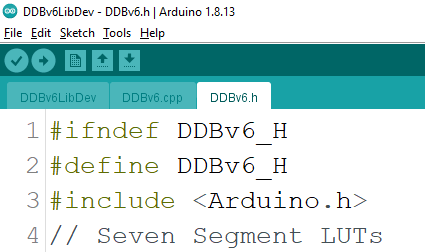
13. DDBv7: The DDBv7XX.h Library
 In programming for the ATmega328P (either the UNO or Nano) you became familiar with predefined constants such as, LED_BUILTIN. Tucked deep inside your Arduino IDE's installation is a library file, called variant.h, that contain this statement (and numerous others),
#define LED_BUILTIN 13
Libraries are an integral part of the development cycle as they reduce development time and ensure greater code accuracy. It would be both instructive and efficient for you to begin to assemble reusable software assets inside your own library of support resources for the DDBv6. Since this is would be a separate file from your specific project applications, you'll need to remember to attach at least two code files when submitting for assessment. Furthermore, since I would have to distinguish between each of your libraries, I would ask that you name your library, DDBv6XX.h where XX are your initials.
Task.
 Create a new project sketch entitled DDBv6LibDev.
- Invoke the New Tab feature (under the Serial Monitor icon in the top right corner of the IDE) and create the file, DDBv6XX.h where XX are your initials.
- Add the definition, #define LED_BUILTIN 8 to your library.
- Within your driver sketch, add the statement #include "DDBv6XX.h" and add statements to capitalize on the library's only asset, to light the DDBv6's onboard LED.
- Add the statement, #define ONBOARDLED (1<<PB2) to your library.
- Add the function, void onBoardLED (uint8_t state) that sets the state of the onboard LED (0-off, otherwise-on) using register-level code.
- Add a Lookup Table (LuT) of base type uint8_t and size 16 to your DDBv6XX.h defining the 7-segment maps for each of the 16 hexadecimal digits. This LuT is to be used in conjunction with your upcoming Pin Change interrupt project.
- Add the function void LEDOn (uint8_t anodePin, uint8_t cathodePin) that turns on an LED, biased as per its parameters. Test this function for a bicolor LED spanning any pair of digital pins.
- Add further definitions and code to your library that you feel would save you development time in the future.
- When you are (temporarily) satisfied with the performance of your local library (DDBv6XX.h), create the folder DDBv6XX in the /libraries folder of your default Sketch folder. Drop in your DDBv6XX.h library.
- Global access to your library is ensured through the use of the #include <DDBv6XX.h> statement.
- Syntax highlighting can be achieved through the use of a keywords.txt file. Here's a lead in that direction: https://spencer.bliven.us/2012/01/18/arduino-ide-keywords/
5. DDBv6: Reset Sources
 You are familiar with the effect of pressing the Reset button on the UNO or Nano, however further optimization is accessible through a deeper understanding of the subtleties the various Reset sources of AVR MCUs. These sources can be detected and subsequently impact how your code chooses to restart.
Chapter 9 of the ATtiny84 datasheet introduces the concept of System Control and, in particular, the Reset Function. The MCU offers four hardware Reset triggers that include: Power On, External, BrownOut, and Watchdog. At the end of this chapter, there is a description of the Registers that can be inspected and manipulated. For our purposes, we'll limit ourselves to a simple distinction between the Power On and External Reset triggers. Page 41 of the ATtiny84 datasheet presents the MCUSR Register, (see: ATtiny84 Register Summary)
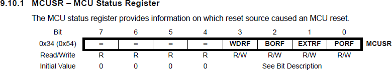
in which the source of a Reset can be identified through the use of flags (bits).
Task.
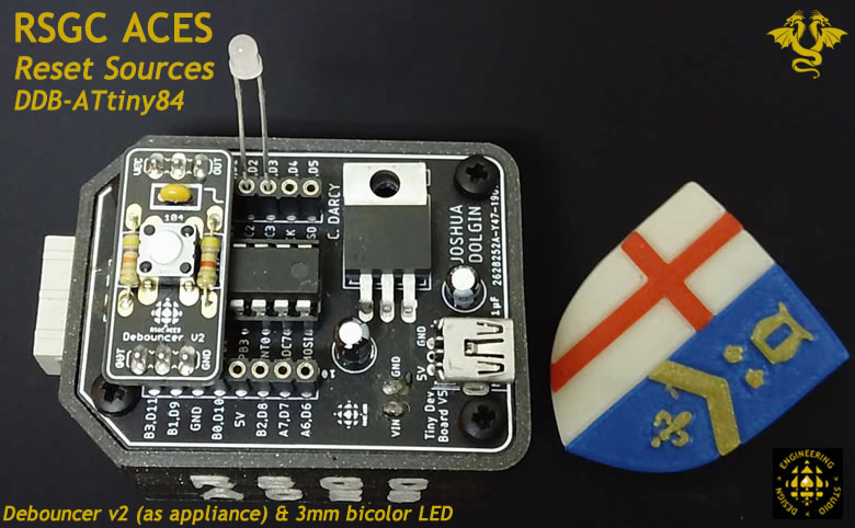
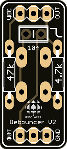 Your Session 5 supplemental parts kit contains an ACES Debouncer V2 PCB. Solder the indicated parts to the board and seat it as an appliance to the DDBv6, so that a falling edge of OUT rests in RESET (digital pin 11; PB3).
- Span your 3 mm bicolor LED across PA2 and PA3. with the longer lead in PA2.
- Open your ongoing DDBv6LibDev project.
- Making maximum use of the predefines included in the iotnx4.h file and register-level code, add statements to your setup() function that will inspect the MCUSR's PORF and EXTRF flags. Invoke your library's LEDOn() function to distinguish between the two sources of the Reset. Show RED for a Power On Reset and Green for an External Reset, triggered by your button debouncer.
- Add resources to your DDBv6XX library as you deem appropriate.
DDP: USB to TTL Serial Cable
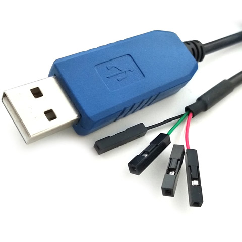
A solution to the benefit of serial streaming to the Arduino Serial Monitor and Plotter from the DDP comes in the form of a USB to TTL Serial Cable from Adafruit (below, left). The basis for this discovery comes in the form of this instructable from OldArkie in which he describes a similar approach from the ATtiny85. The image below, right (click to enlarge) is of a dynamic application of a thumb joystick in a DDP running a sketch (SerialOutputDDP.ino) that streams the 2D coordinates to a Processing application (CircularTrigFunctions.pde) developed to introduce students to the true origin of the six trigonometric functions: The Circular Functions. USB cable connections to the DDP can be determined by looking closely at the photo. The White 5V wire is not connected.
I'll provide a demonstration in class on the resumption of classes after the March Break 2020. Both sketches are available from DDP's GitHub repository.
| Adafruit USB-to-TTL Serial Cable #954 |
DDP Control over the Processing Circular Function Sketch |
 |
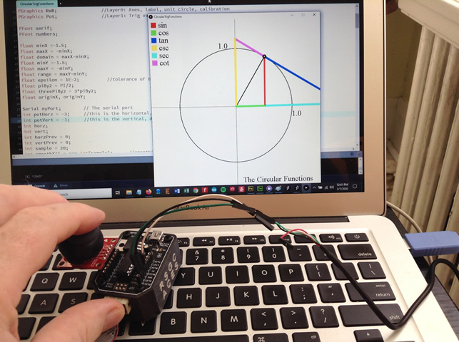 |
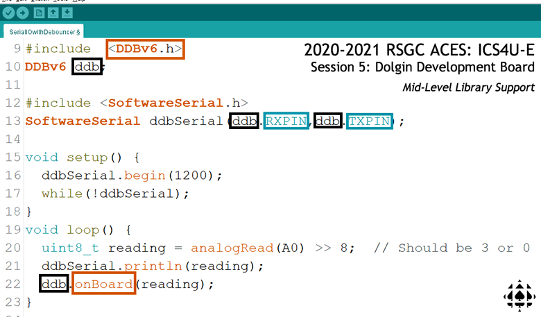
6. DDBv6: SoftwareSerial
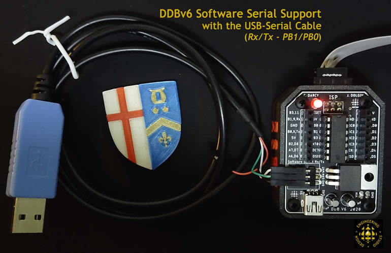 Until such time as the DDB supports hardware USB-to-Serial communication (Version 8?) we make do with software serial support. The USB-TTL Serial cable from Adafruit that you have been provided with permits your DDBv6 to transmit data to your Arduino IDE's Serial Monitor and Plotter.
Task.
- If they are not defined already, add the following definitions to your DDBv6XX.h library,
#define RXPIN 9
#define TXPIN 10
- A SoftwareSerial object can now be instantiated in the form of,
#include <SoftwareSerial.h>
SoftwareSerial ddbSerial(RXPIN, TXPIN);
- Confirm the identification of the Reset Sources explored in the previous exercise by writing a specific String to the Serial Monitor.
Concept: ATtiny84 Interrupts
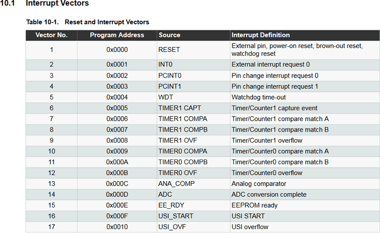
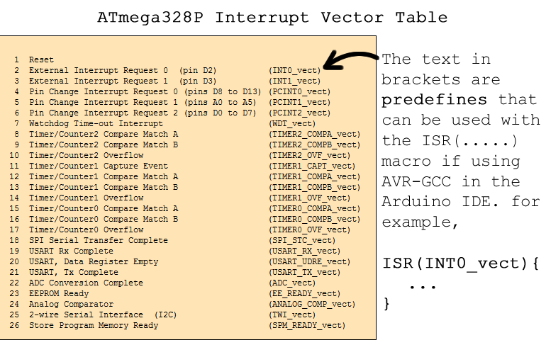
Interrupt-driven programming strategies can provide a more efficient approach for responding to asynchronous events. Chapter 10 of the ATtiny84 datasheet, Interrupts, introduces the MCU's Interrupt Vector Table that appears to the right. The order in which they appear in the Table implies priority should multiple events happen simultaneously.
ATtiny84 External Interrupt
As can be seen, a Reset event is assigned the highest possible precedence, followed by a (single) External Interrupt (INT0; the ATmega328P has two and the ATmega2560 has eight!), and so on. A design mistake I made on the DDBv6 was to attach the onboard LED to digital pin 8 (PB2). Since this is the same pin that supports the INT0 function, the feature was rendered dysfunctional. In DDBv7, the onboard LED was relocated to digital pin 4 (PA4/SCK) restoring the use of INT0.
In class, we'll temporarily switch back to the UNO/Nano and confirm your register-level coding of its INT0 or INT1 interrupt capability through the use of the debouncer. We'll be sure to make maximum use of the 328P's header file of predefines: iom328p.h. Also, since the Arduino IDE employs the avr-gcc compiler, the 328Ps Interrupt Service Routines (ISRs) use the following Vector Table syntax for naming the ISRs,
Page 71 of the ATmega328P datasheet provides Register level details associated with the ATmega328P's External Interrupt manipulation.
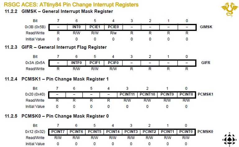
7. DDBv6: Pin Change Interrupt
Chapter 11 of the ATtiny84 datasheet discusses this MCU's functionality with respect to external Pin Change interrupts. Whereas specific bits can be configured for 'sense control' on the single External Interrupt INT0 (PORT B.2) to sense rising, falling, change, or low signal conditions, only change triggers a Pin Change Interrupt. However, the good news is that any digital pin can be conditioned as such. The applicable registers, bits, and flags are summarized below.
Task.
- Create the project, DebouncerWithPCInts.
- With your up-to-date DDBv6XX library sitting in the \libraries folder of your Arduino Sketchbook folder, add the #include <DDBv6XX.h> directive to this sketch for your first 'official' use of your library's assets!
- Add additional code to the project that implements register-level code to configure your button debouncer to trigger an interrupt on any pin of your choosing. The onboard LED should light for 500 ms as confirmation.
8. DDBv7: Morland Bargraph v3
9. DDBv6: Rotary Encoder
 As discussed in class, encoders are devices that can map digital signals to binary form. Rotary encoders can present relative changes in angular position to binary form that can be read by MCU to determine counts, or even rotational speed, when applied over the time domain. Here's a short video highlighting the output of an inexpensive rotary encoder on a KY-040 breakout board from Amazon, Rotary Encoder with Bicolor LEDs.
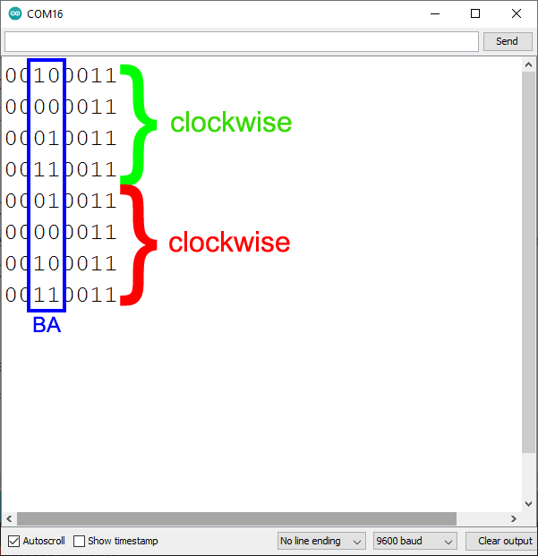
In the Serial Monitor capture to the right, rotary encoder outputs A and B were configured as pin change interrupts on digital pins 4 and 5 (PD4..5), respectively. The port PIND was read and echoed after one clockwise rotation between detente positions followed by one counterclockwise rotation. The Gray Code sequence is clear as should be the strategy to detect the angular direction.
Task.
- Using the instruction and assets provided you, develop Pin Change Interrupt client code that will monitor your rotary encoder in the form of clockwise (increasing) and counterclockwise (decreasing) counts.
- Using your MBv3 as the display device echo the encoder count continuously.
10. DDBv6: CharlieStick
 References
- ATmega328P Datasheet. See Section 36 starting on page 612.
- ATmega328P Include file: iom328p.h
- ATtiny24/44/84 Datasheet. See Section 24 starting on page 182.
- ATtiny24/44/84 Include file: iotnx4.h
- Search for evidence within the ATtiny84's iotnx4.h file that confirms the information in the adjacent Data Memory Map graphic.
- After digesting the previous references you'll appreciate that the header file simply consists of hundreds of
#define compiler directives that provide aliases for the specific AVR MCU registers and bit-within-a-byte numbers.
- Last fall, in Project 3.2 you were asked to explore Charlieplexing and tasked with implementing our new charlieplexed SimonStick. as Project 3.2.1. As a followup task, Project 3.4.2 asks that you adapt your previous sketch by maximizing your use of Register-Level coding strategies and other
#defines from the header file to have your SimonStick function as a VU meter for the TMP36 temperature sensor.
 CharlieStick (Register-Level Coding)
Note: Both devices are expected to be implemented as DDP appliances. You'll have to think strategically for this.
 Create a DDP folder within your Arduino sketch folder and condition yourself to placing all of the sketches developed for use on the platform in this folder.
- Run through a familiar sequence of devices and high-level programming practices to get acquainted with our new environment. Provide evidence in your first DDP DER entry that you have successfully implemented the following three trials: the single LED blink sketch, the Schaffer Traffic Light, and the Morland Bargraph. For the latter, you'll note that the power supply and digital pins of the ATtiny84 have been broken out in a manner perfectly suited for this device. Be sure to highlight this in your Report. I suggest you showcase the following four Morland Bargraph capabilities,
 Simple, recognizable binary sequence or alternating pattern
 Shift out
 0xFF and demonstrate a 'breathing' bargraph by placing a signal on the 595's output enable pin
 Review Adafruit's TMP36 terrific tutorial. Now, what's great about the DDP is that without support of the Serial Monitor, we're (somewhat) blind. However, our Morland Bargraph is an output device that can tell us a great deal if we exploit it correctly. So, wise ACES will, first, familiarize themselves with the TMP36 in a more 'informative' environment. Wire the TMP36 from a breadboard to your Arduino UNO and explore its output with the help of the Serial Monitor. OK, with a better understanding of the device, insert it into a strategic location on the DDP and project the result of an analog reading of the sensor on your bargraph over an appropriate thermal range of your fingers while pinching the device. You can either present the raw readings or tailor it as VU meter with a little math. (
map() and constrain() are handy functions for this application as is bit-shifting). Some other creative and inspiring exercise of your own choosing. Look in your kit and come up with something compelling.
Finally, pack these four Morland Bargraph exercises into a single sketch with some strong code design decisions. Note, the mark you will receive will be based, in part, on how unique your code is from that of your peers.
11. DDBv6: Power Management
The ATtiny84's Interrupt Vector Table continues to serve as a guide to strengthening your hardware, software, and design skill base. Next stop: Watchdog time-out interrupt support for the power-down sleep mode.
As a context, it is not difficult to imagine a remotely-situated, solar-powered, MCU-based sensor device that collects (and possibly transmits) data to a centralized location. Understandably, optimum use of power would contribute to its viability and sustainability. This segment provides some insights into how some aspects of such a prototype could be implemented to conserve power between readings.
One video I encourage you to watch is Kevin Darrah's Low Power Arduino! Deep Sleep Tutorial. This presentation contains applicable material for this investigation.
I've partitioned this investigation into two development stages.
Dolgin Development Terminology
 DDB. The Dolgin Development Board is the assembled PCB that provides ACES with our own MCU-prototyping motherboard based on the ATTiny84, developed by J. Dolgin (ACES ' 20, Waterloo '25) from an earlier concept by J. Corley (ACES '19, Queen's '23).
Appliance. An Appliance is an ACES' term for any PCB-based device that is inserted vertically into a SINGLE female header on either the UNO or the DDP. The Schaffer Traffic Light (STL), the Morland Bargraph (MB) and the CharlieStick, are three previous examples.
Shield. A Shield is the conventional Arduino term for a PCB-based device that spans BOTH female headers, horizontally, on the UNO. ACES have adopted this term in reference to a device that spans both headers on the DDB. In late 2019, two DDP Shields were developed for ACES to continue to develop their MCU prototyping skills. By the end of the term, after working extensively with these two shields, every ICS4U ACE will have the opportunity to add to the inventory of our DDP Shields through the creation of their own, original, Legacy Shield for future ACES to benefit from. As of Spring 2021, the ACES collection has increased to include five shields: Intersection, ADC, Universal 1, Universal 2, and Equalizer.
DDP. The Dolgin Development Platform is the ACES' term for any number of shields stacked on the DDB, installed in our 3D-printed custom base, all functioning as a coordinated unit.
12. DDP: Intersection Shield
 For your first shield exposure our Schaffer Traffic Light (STL) gets a significant upgrade in the form of 2-way Intersection simulation with countdown displays in both directions. The device can be thought of a Finite State Machine (of the Moore variety) in which the state transitions are to be triggered through WDT Interrupts you were acquainted with from a previous section.
- Watch this clip of the simulation, DDP: Intersection Shield (1:08)
- Download the EAGLE Files for this Shield and review the connections thoroughly. Take as much DESIGN information into consideration as you can for your similar Legacy Shield effort later this year. Since this Shield is densely populated, there was not as much room for silk screening.
- Review the Shield's schematic and dig deeper into the EAGLE files, if necessary, to determine the pin assignments.
- The Intersection Shield uses two, narrower-pitched, 7-segment displays (2mm pitch, LA-301VL).
- In developing code to match the video sequence and timing as closely as possible you'll stretch your DDBv6XX.h library use, apply maximum register-level use and use the WDT interrupts to as far as you can.
- Develop the code in two stages. The first will ignore the countdown timers, opting to only have the WDT interrupt schedule the state transitions. Define a state table (array of structs) to support efficient implementation No long if..else ladders here, thank you.
- With the transitions functioning, the second stage implements the countdown displays (7→0) within the two applicable states.
- Comment your MODULAR, EFFICIENT, COMPACT code, extensively.
| DDBv6 |
Intersection Shield v2 |
|
|
14. DDP: ADC: Successive Approximation
 Of all the features that microcontrollers offer, a strong case could be made for Analog to Digital Conversion being its most important function. After all, the ability to capture real world data and digitize it for manipulation, transmission, and storage purposes is an undeniably critical feature within our modern world. Although the AVR line of 8-bit MCUs offers a 10-bit onboard DC unit that we've exploited for a number of purposes, what if our needs called for either a higher or lower sampling accuracy? A deeper understanding of how the ADC function works is called for should we wish to build our own ADC unit.
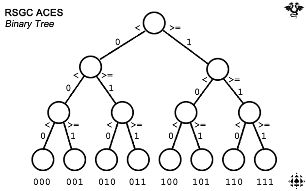
An informative base from which to mount our investigation might start with a somewhat familiar binary tree. As a child you might have engaged in a guessing game in which a series of ranked guesses with a response of either lower or higher could lead you to your target. Indeed, this approach could lead to a conversion method from decimal to binary as suggested by the labeled paths.
Day 1.
Previous projects over the years have exploited the use of operational amplifiers as comparators. The LM741 and dual LM358 are common examples that two voltage levels on their non-inverting and inverting inputs, outputting a 1 or or 0 depending on whether the non-inverting voltage is greater than the inverting input, and a 0 otherwise. The ATtiny84 has (as other AVR MCUs do) a built in comparator that will provide the foundation for week of ADC/DAC exploration.
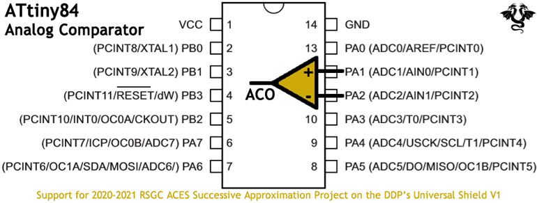 A review of Konde's ATtiny84's pinout diagram reveals the location of the Analog Input (AIN0 and AIN1) pins.
- A review of the ATtiny84's Interrupt Vector Table suggests that upon completion of an Analog Comparison an interrupt is generated (#13).
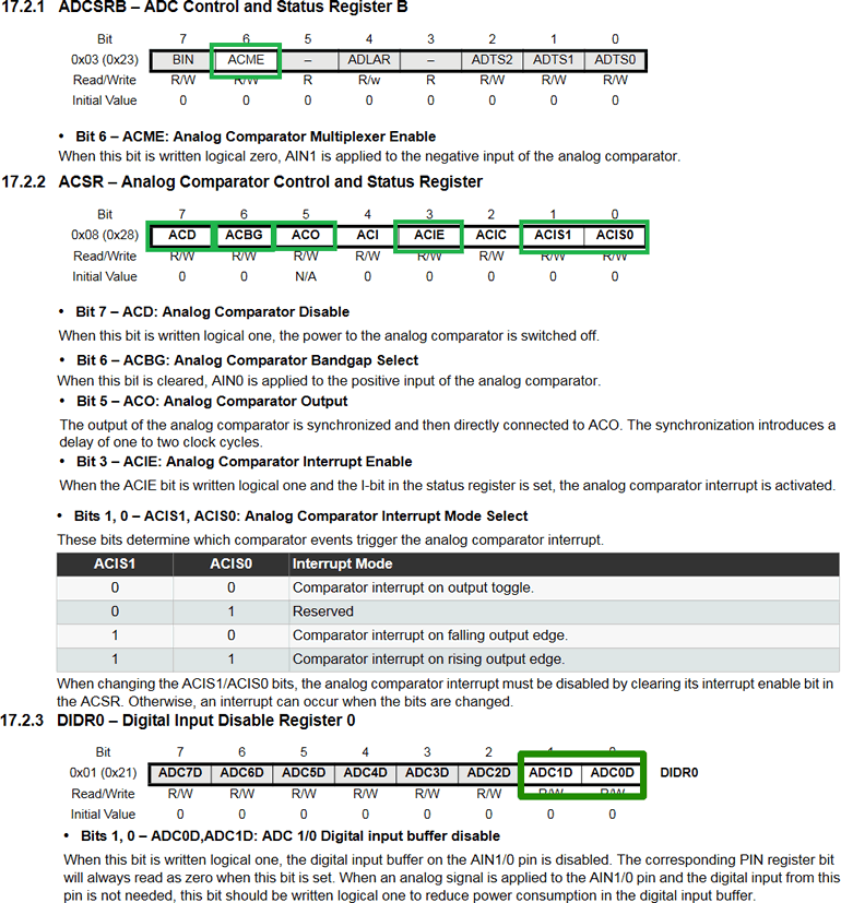
- Chapter 17 of the ATtiny84 Datasheet offers a three-page summary of how the Analog Comparator functions and the registers required to configure it for specific use. We'll review this in class.
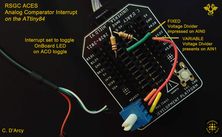
- The photo below shows the USv1 with a 2.5V reference voltage impressed upon the positive (non-inverting) input AIN0. A variable voltage from the trim potentiometer is applied to the negative (inverting) input AIN1.
Day 2.
- A review the AC's block diagram summarizes the architecture of the function. Register bits that need to be configured for our purpose are highlighted in green.
- The AC's applicable registers and flags have been extracted and summarized for you, below the block diagram. Review these settings in preparation for the code we are about to develop together.
- Create the sketch ACInterrupt.ino. Develop and test code that will toggle the DDBv6's onboard LED every time the Analog Comparator Output changes state.
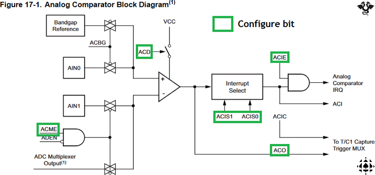
Day 3.
TBD...
15. DDP: Legacy Shield
 A quotation, attributed to the Greek statesman, Pericles, is apropos,
"What you leave behind is not what is engraved on stone monuments,
but what is woven into the lives of others."
ACES' tradition reflects a popular culture trope in which Master Craftsmen Make Their Own Tools. A quick review of the ACES PCB Archive supports this claim. In this latest attempt to enrich the engineering experience of the ACES that follow, you have the opportunity to add to the inventory of DDP Shields. Coupled with this task is the opportunity to weave your name in the minds of future ACES as Bagga, Benson, Schaffer, Morland, and Dolgin have done in yours.
Task.
-
Reflect deeply on a previous ACES' project or set of components that we explored (or wished we had) that would enrich future ACES understanding of a concept. Keep in mind the simplicity, availability of parts, form, and cost of such as design. The designs with the greatest potential to result in production are typically the simplest, least expensive, most flexible and easily adaptable to the broadest range of applications.
- Your familiarity our current shields frames the constraints placed on the possible design of your Shield, not the least of which are its dimensions. Furthermore, by the time ACES are ready to assemble their DDP Shield, you can assume they have SMD/T experience.
- Your Session 6 supplementary parts kit contained all the components to assemble both the #1 (SIP) and #2 (DIP) DDP Universal Shields. You are asked to solder both of these up and use either them as the base for your functioning Legacy Shield prototype.
 If you have not done so already, create EAGLE projects from the .sch and .brd files available from our RSGC ACES' Dolgin Development Project repository. After settling on your idea, download and copy the Shield files (Intersection and/or ADC) that are a better fit with your plans, remove component you do not need and start designing. You only need to ensure your board outline remains identical, as do the positions of the two 1×8 headers that connect to the DDP motherboard.
- Be sure to use the ACES SMD/T EAGLE resources available from the top of our course page to expedite your results.
- By the deadline, attach four files (DER.docx, .sch, .brd, and .cam ) to an email to handin under the Subject Line: DDP: Legacy Shield.
- Ideas? TTC Line 1 (Coding skill), Breadboard Shield (Prototyping), Sensor Shield (Testing), 0.96 OLED Display, Electret Mic, Universal IR Remote (IRremote library supports the ATtiny84 (digital pin 6)), Motor Shield (DC Hobby? Servo? Stepper?), etc.
Results
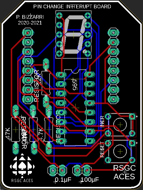
| SA: Serial Binary Game |
PB: Pin Change interrupts |
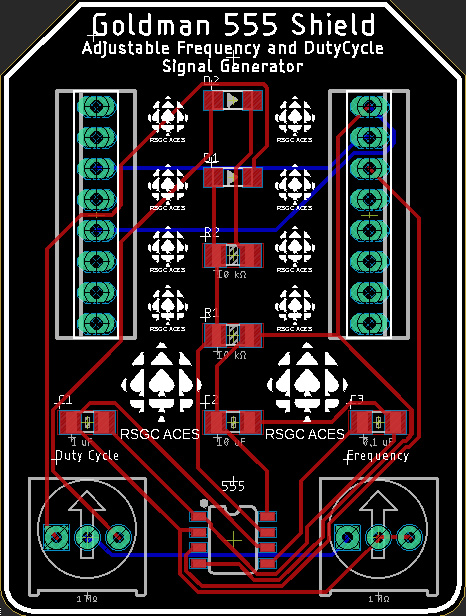
AG: Signal Generator |
 |
 |
 |
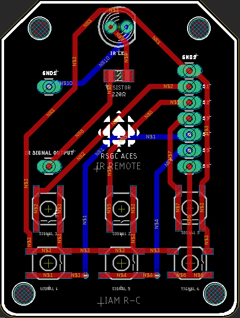
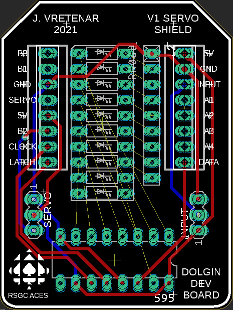
| LRC: IR Remote |
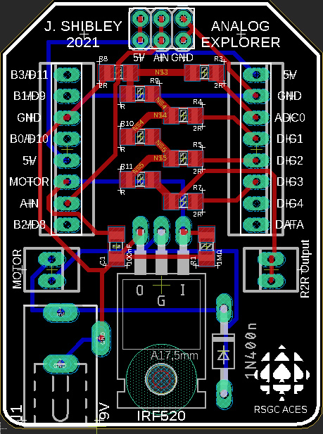
JS: Analog Explorer |
JV: Servo Shield |
 |
 |
 |
7. DDP: AVR Assembly Language Programming
7.1 References
7.1.1 GPIO Port Summaries
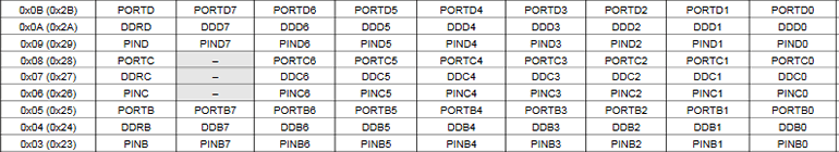
7.1.1.1 ATtiny84
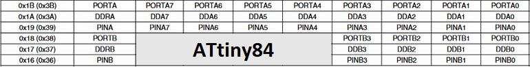
7.1.1.2 ATmega328P
7.1.2 Summary: AVR Assembly Instruction Set
7.1.3 Detailed: Online AVR Assembly Instruction Set
7.1.4 Full Manual: AVR Assembly Instruction Set
 7.2 Exercises
7.2.1 Inline (8-bit) AVR Assembly (within the Arduino IDE)
In our first few AVR assembly exercises you will explore how the AVR-gcc toolchain permits the interspersing of assembly language statements amongst Arduino C statements through the use of the asm () macro. This blog offers a primer...The following video provides a good foundation for AVR Assembly concepts in a little more detail than is required at the moment but, nevertheless, is highly instructive: Intro to Arduino Inline Assembly
7.2.1.0. The Fastest! Blink
In a previous exercise you successfully confirmed that setting a bit in an AVR Port's PIN register, toggled the corresponding bit in its PORT register, leading to the fastest way to blink an LED. In this first exercise we'll perform the same task, in assembly language.
Task.
- Insert an LED into your DDP spanning A0 and ground.
- Within an
InlineAssembly folder, create a New Project called BlinkInline.
- Within your
setup() function , add an asm volatile () macro that declares PORTA, pin 0, for output.
- Within your
loop() function, add an asm volatile () macro that writes 1 to PINA, pin 0.
- Using the builtin
delay() function add a 1 second delay between loop iterations.
7.2.1.1. (All Assembly) Delay
 A clock cycle is a tick of the MCU's oscillator. The source of these ticks typically comes from the MCU's external crystal or internal RC clock.
As you can imagine, the benchmark measure of the efficiency of any code sequence rests with determining the number of MCU clock cycles (or simply clocks) it takes to execute, not the absolute amount of time the code takes to execute. Courses in your university Comp. Eng, program will require you to explore this this so let's get a simple taste, now. Further reading: AVR-libc Benchmarks
The delay(ms) function is handy, but unproductive, as all it does is waste clock cycles. Nevertheless, exploring an 'All AVR Assembly' equivalent to the delay(ms) function is instructive for our ends. So, although the previous exercise confirmed that inline assembly and high-level C can coexist, this exercise allows you to explore replacing the high-level delay(ms) function altogether through additional assembly instructions inside our loop() function's asm volatile( ) macro. In doing so, we'll also acquaint ourselves with a few more AVR instructions.
Task.
- Review the AVR Instruction Summary I've posted online. The last column indicates the clocks for each instruction.
- Follow this link for a more comprehensive AVR Instruction Reference.
- Q: How many clock cycles does the
sbi instruction consume in execution?
 Review this handy code generator calculator for wasting AVR clock cycles offered by Bret Mulvey. (Wise ACES will right-click the page and review the Javascript source code to deepen their understanding of these important code techniques) An inspired JS enhancement was made by T. Morland, ACES' 18, (of Morland Bargraph fame) which I'll explain in class. You'll also find this utility by click the DELAY link at the top of our course page, as you'll want to exploit its value, often.
- Q: Load the AVR Delay Loop Calculator and go to the last text input box (cycles), enter the number 100, and press go. Select avr-gcc and examine the assembly code. Explain why the assembly code is correct (for this value) in terms of wasting clock cycles. Try additional multiples of 100 up to 800. Any comments? Conclusions?
- Complete the entries to generate an equivalent sequence of Assembly instructions as a replacemnt for
delay(1000). Again, choose the avr-gcc syntax for now.
- Load your
BlinkInline sketch from the previous class and remove the call to the delay(1000) function. Copy the auto-generated code from the previous step and insert it into your loop() function's asm volatile( ) macro.
- Listen closely to the additional explanations in class to have your code run as expected.
7.2.2 Standalone (8-bit) AVR Assembly Coding (within the Arduino IDE)
Reference (unnecessarily complicated but informative, nonetheless): https://rwf.co/dokuwiki/doku.php?id=smallcpus
 The Arduino IDE offers painfully few tools for the aspiring assembly language programmer to develop a skill set but it has one important thing going for it: familiarity. Make no mistake, confidence, coupled with steady productivity and reasonable success, are required to sustain interest in the challenge of low-level coding and, so far, you're making SUBSTANTIAL progress.
So, let's keep the hardware task the same (fastest blink of an LED) but strip away the cumbersome " " and \n from inline assembly to write clearer, standalone, AVR assembly code.
7.2.2.1. The Fastest! Blink
 Within a folder called
 StandaloneAssembly, create a first project called FastestBlink.- (Now, this step will seem weird...) Delete ALL comments and code from
FastestBlink.ino leaving the file completely blank. (an informative action would be to compile (verify) this empty file and read the diagnostic error messages it produces. Remember, all the code you have ever run in the Arduino IDE operates within the C driver shell main.cpp)
- So, if we hope to have any of our own code run within the Arduino IDE, we require, at the very least, both a
setup() and loop() function. We'll now provide these functions in Assembly!
- Our standalone assembly code will be placed in a completely different file, within the project, with the extension,
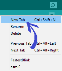
.S (Note: it MUST be a capital S). Look to the top right corner of the IDE, click on the dropdown button, select New Tab and, in the text box, label the new file, asm.S. (Note: you could call it anything you want but let's keep it consistent for today)
- Now, enter the code below in the
asm.S. file. The .global assembler directive is one of many that assists the toolchain with the creation of the final executable. Functions in assembly language are simply labels. Furthermore, it should be obvious now that they terminate with a ret statement.
.global setup
setup:
	ret

.global loop
loop:
	ret
- You can now add the familiar assembly statement to the
setup function, free from the " " and \n syntax required in inline assembly. Comment appropriately.
- Additionally, add the familiar statement to your
loop function. Comment appropriately.
- For our kill function, a
.global directive is not required as this function requires only local access (ie, not visible to other files in the project that will be linked together). Return to our AVR Delay Calculator to obtain assembler code for the body of our kill function that will simply waste 1s worth of clock cycles. Comment appropriately.
- Add opening comments within your
asm.S file, upload. and admire!
- Note 1. The Auto Format feature does not apply to assembly code. You must do this by MANUALLY.
- Note 2. EVERY assembly statement deserves a meaningful comment. Get used to it.
- Note 3. Compile this code and COMPARE the amount of program storage space it requires to the standard
File>Examples>Blink sketch.
7.2.2.2. Schaffer Traffic Light
In this second standalone AVR Assembly exercise we return to the venerable STL to continue to expand our knowledge base of instructions. Setting (or clearing) an individual bit od a PORT is handy, but typically you'll want to affect multiple bits at a time. For these purposes you'll need the in and out instructions.
Place your Schaffer's Traffic Light into DDP pins A2..A0 + GND.
(conveniently, the Intersection Shield works just as well for these exercises)
7.2.2.1.1 Version 1
- Within your
AssemblyStandalone folder create the project STLv1.
- Clear the
STLv1.ino file and add an STLv1.S tab.
- Insert the
.global functions setup and loop.
7.2.2.1.2 (Improved) Version 2: AVR Assembly delay(ms) Function
Rather than entering and exiting multiple asm volatile () blocks, Version 2 accomplishes the same result with a single asm volatile () block by replacing the Arduino C delay(ms) function with an assembly function that does the same thing (waste clock cycles).
- Save your successful
STLv1 project as STLv2.
- Review the Mulvey/Morland utility for determining just how many cycles to waste. Since we're exploiting the ATtiny84's internal 8 MHz RC clock, enter the parameters to generate code for a 1s delay (we'll use the avr-gcc version for this sketch).
- This auto-generated code introduces you to a few new assembly instructions (ldi, dec, brne).
- If this 1s assembly code sequence could be structured to reflect a function, it could simply be called n times to waste n seconds! This will introduce the rcall and ret assembly instructions.
- Within a single
asm volatile () code block in the setup() function, run the STL continuously for same the 3s-1s-3s delay sequence.
Seven Segment Counting
To strengthen your skill set, I have carefully developed an integrated set of increasingly-complex projects based on the DDP and the ADC Shield especially for you; the 2019/2020 ICS4U class. It's imperative that you take the concepts that you have been taught, acquire these skills, and prove to yourself you can handle a degree of complexity.
 To start, Using the AVR Assembly knowledge gained so far, in particular our Data and Labels lesson, you are asked to present single digit counting, either on a standalone 7-segment display or, preferably, on your ADC Shield. I have prepared a video of what I expect you to develop:
Seven Segment Counting Support Video
I have broken down the necessary steps below to such a degree that anyone with even the slightest bit of motivation and interest in preparing for the challenges that lay beyond RSGC should be able to fulfill.
Task.
- Create a project called
Shiftout7Segment.
- Within the Program Flash section (
.cseg or .text), define a 10-element array of segment maps of the form (0Babcdefg0). This will require the use of the .DB or .BYTE directives.
- Declare start and end labels, before and after your array (aka. Lookup Table or LUT).
- Your code should assign the start and end labels to the 16-bit X and Y (pointer) registers as I demonstrated thoroughly last class in the Data and Labels lesson.
- Next, turn on the active 7-segment display by ensuring ground access for the display, If doing this on a single CC display, simply wire pin 3 or 8 to ground. If using the ADC Shield, the rightmost display as shown is grounded by setting
PA4 (which is connected to the base pin of its low-side transistor). These assignments can be determined from theADC Shield's silk-screening.
- Your code will undertake a continuous loop with the Z register pointing to the same starting LUT address as the X register and advancing by 1 (autoincrement) until it reaches the Y address. With each iteration, the value from the LUT (pointed to by Z) is shifted out to PORTA using the MSBFIRST direction.
- Insert a 1 second delay between digit presentations.
- The result is a continuous display of the digits from 0-9, repeatedly, as shown in the video.
Be prepared for Monday in the event you get randomized for a Show&Tell.
PoV on the ADC Shield
 This project is a consolidation of previously undertaken AVR skills, investigations, and projects. The first DDP Shield you worked with, the ADC Shield, has a set of four, fully-resisted, 7-segment displays, accessible through the use of the onboard 595 shift register, using a Persistence of Vision (PoV) scheme. The PoV is enabled as the ATtiny84's port pins
 PA1..PA4 are tied to the respective base pins of the four, low-side NPNs that provide ground access to each of the CC displays, in turn.
Task.
- Create the project:
PoVontheADC.
- Through the use of labels and the
.DB (.BYTE) directive, your code should define an 10-element array of segment constants within the .cseg (.text) section, defining the state of the LEDs in the order 0Babcdefgx.
- Hard code a value between 00 and 99 into Program Flash with the
.db directive (or .byte if in the Arduino) to be displayed on the ADC Shield using your shiftout function from a previous project by the same name.
- Shifting out should be undertaken with
MSBFIRST if the segments are defined as indicated in the previous step.
- The correct
DATA, LATCH, and CLOCK equates can be found in a recent post to the ICS4U Conference.
- As stated, the PoV strategy is accomplished by repeatedly signaling the base pins of the transistors to pull the CC displays to ground. The base pins are attached to
PA1 through PA4.
- Document and format your code to a standard that reflects the handouts I've prepared for you.
- Bonus: For the motivated amongst you, I encourage you to take this project up a level. I could have asked for a 16-element array of segment constants (0-F), asked you to hard code a value between 0000 and FFFF, and requested a 4 digit PoV display.
Attach JUST two files ONLY: DER.docx and either main.asm (or PoVontheADC.S if you develop within the Arduino IDE) by the deadline.
 Pseudocode for this Algorithm...
- Define a 10-element segment Lookup Table (LUT) in Flash (same as previous task)
- Assign to
number the two-digit value (eg. 99) to be displayed
- Reserve two bytes of storage in SRAM for the as-yet-to-be-determined tens and units digits of
number
- Define a register
count to hold the tens digit. Initialize it to 0
- Assign to
Z the address of number
- Load
r16 with Z (number) with the lpm instruction
- Subtract 10 from
r16
- If the result is less than 0, (the tens digits has been determined:
count) advance to Step 10 (brmi)
- Increment
count and go back to Step 7
- Store
count in the first of two SRAM storage bytes reserved in Step 3 (sts)
- Add 10 to
r16 (this is the units digit) and store to the second reserved byte in SRAM (sts)
The two digits have been separated, stored in RAM bytes, and ready for PoV display...
- Load
Z with the starting address of the LUT
- Load
r16 with the units digits from SRAM (lds)
- Add
r16 to ZL to have it point to the correct segment map in the LUT
- Load
n with the value pointed to by Z (lpm)
- Turn off the tens display (DIG3) (
cbi) (remember, we need to reduce ghosting)
- Call your
shiftout function
- Turn on the units display (DIG4) (
sbi)
- Pause for a PoV-suitable interval (see Lesson 69 on our course page)
- Load
Z with the starting address of the LUT
- Load
r16 with the tens digits from SRAM (lds)
- Add
r16 to ZL to have it point to the correct segment map in the LUT
- Load
n with the value pointed to by Z (lpm)
- Turn off the units digit (DIG4) (
cbi) (remember, we need to reduce ghosting)
- Call your
shiftout function
- Turn on the tens display (DIG3) (
sbi)
- Pause for a PoV-suitable interval (see Lesson 69 on our course page)
- Go back to Step 12
7.2.2.4. Morland Bargraph Array Presentation
To be developed...
7.2.2.5. CharlieStick
To be developed...
7.2.2.6. CharlieArray
To be developed...
To be developed...
7.3 Standalone Assembly (Atmel Studio 7)
Yikes! :)

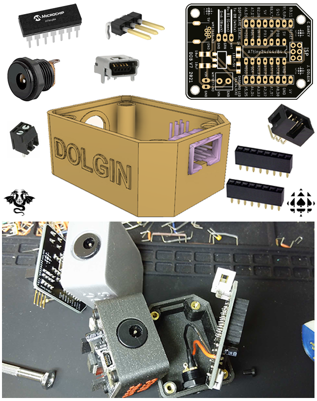
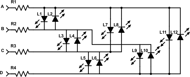
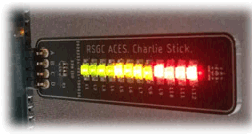
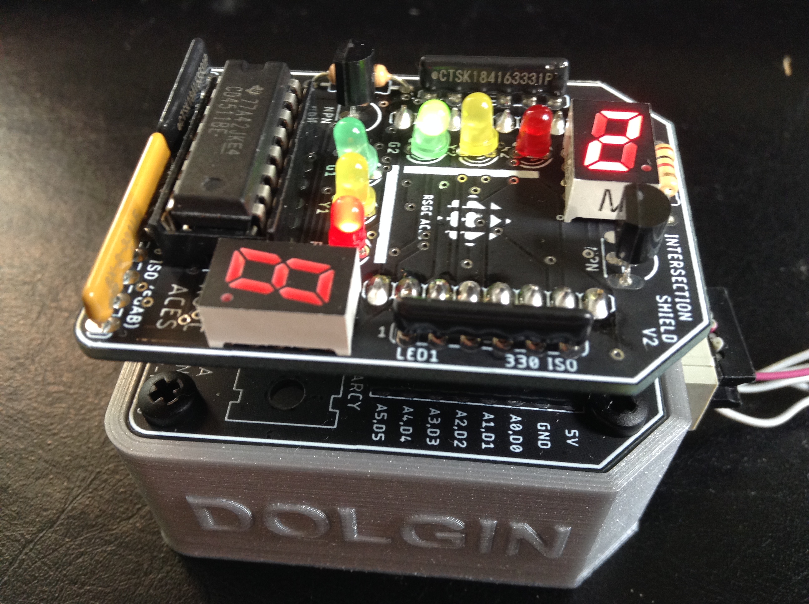
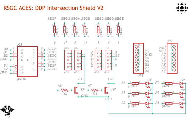
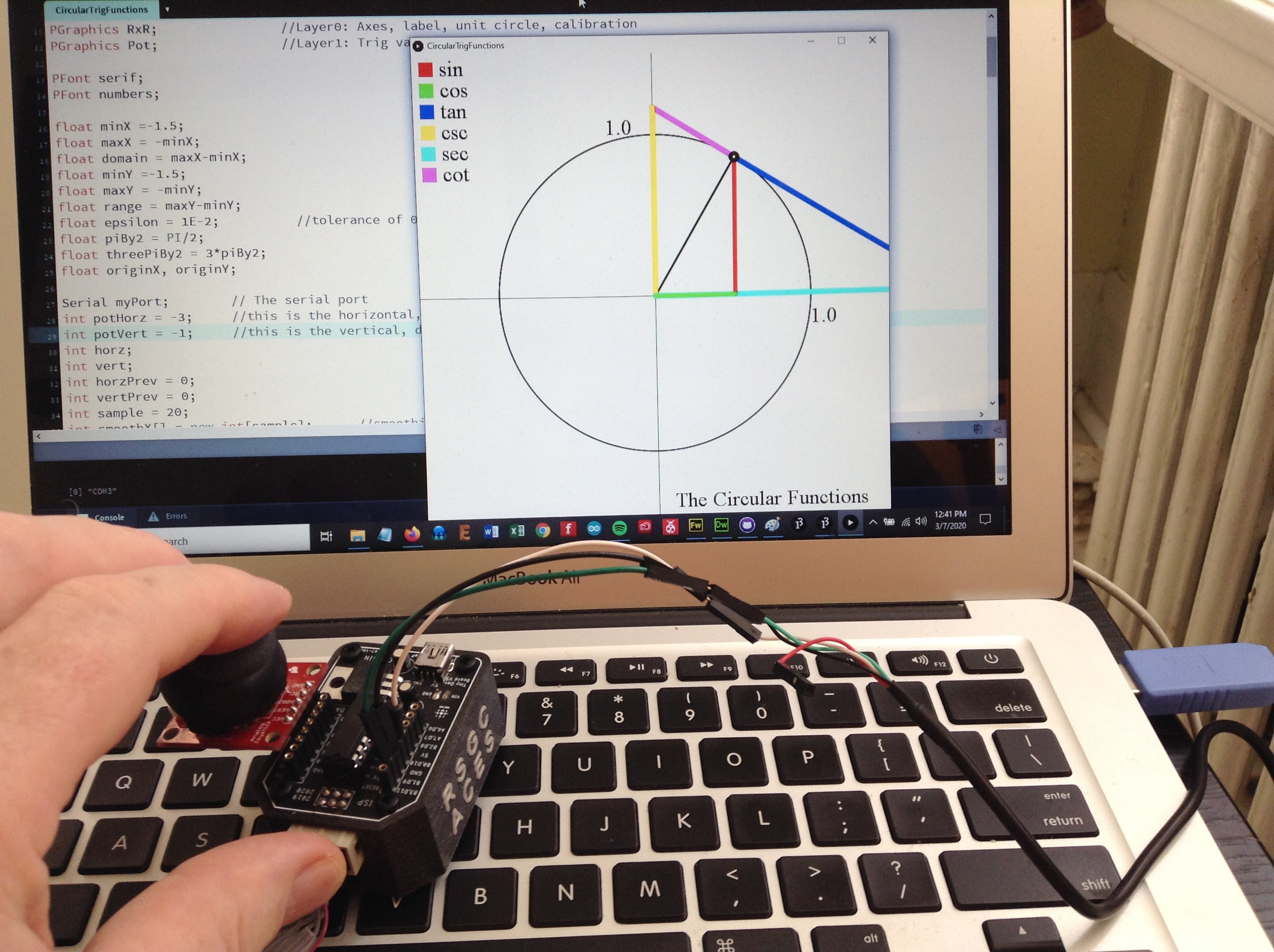
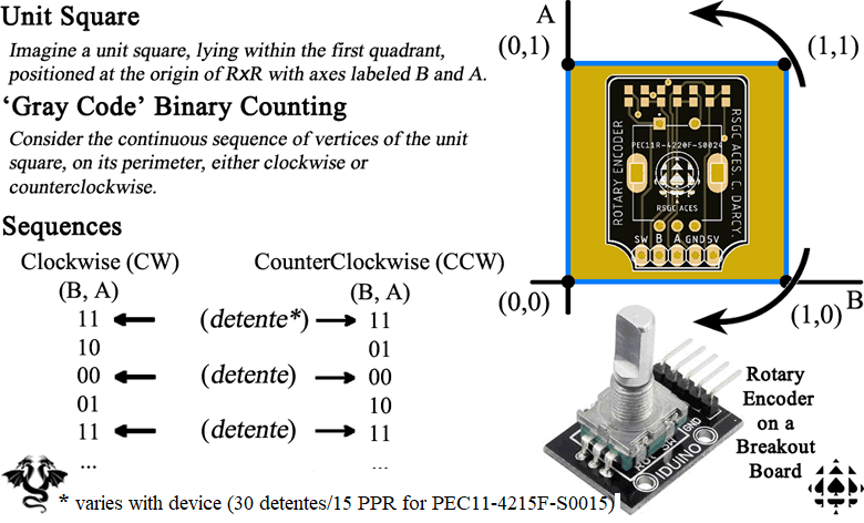
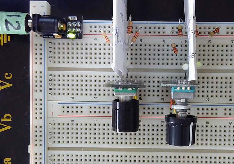
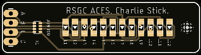


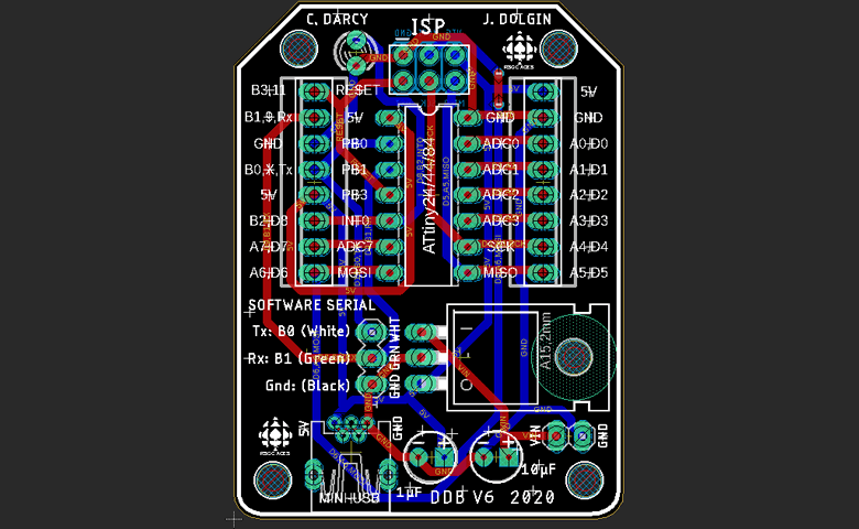
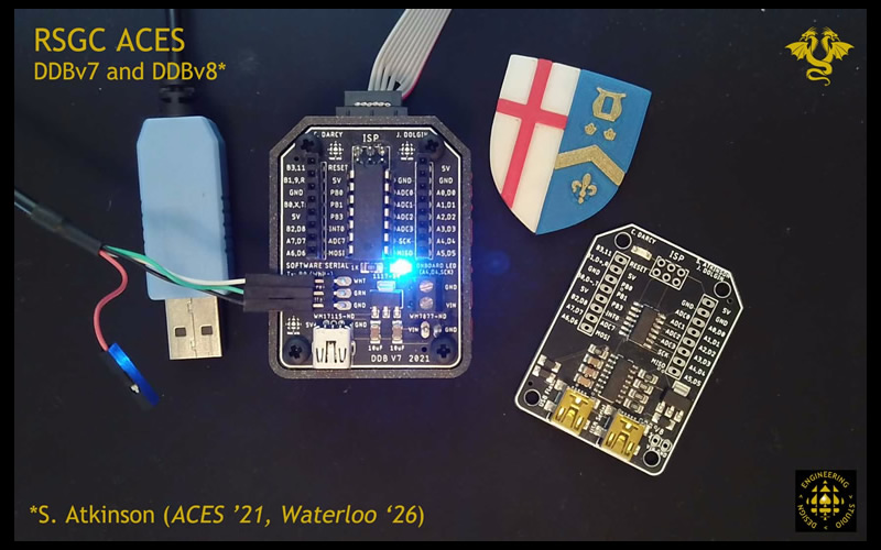
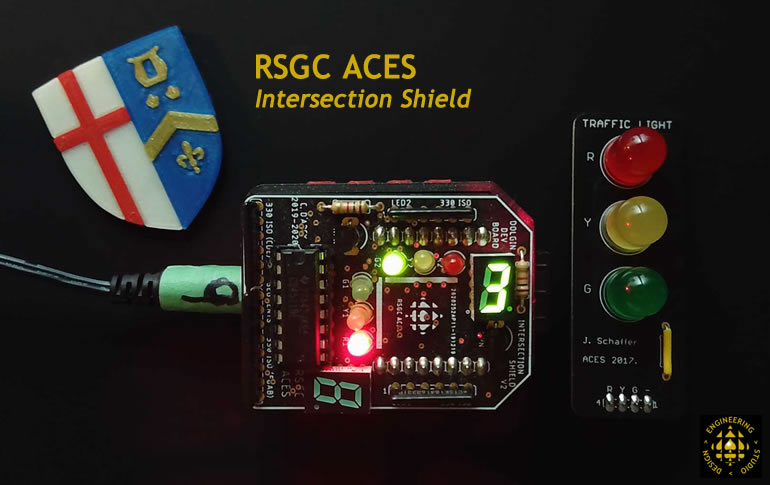