 It is virtually impossible to trace the true origin of any significant achievement as even its creators may not fully understand the source of the inspiration(s) that led to their breakthrough. However, for this gem, I'll pick up the thread in the Spring of 2018...
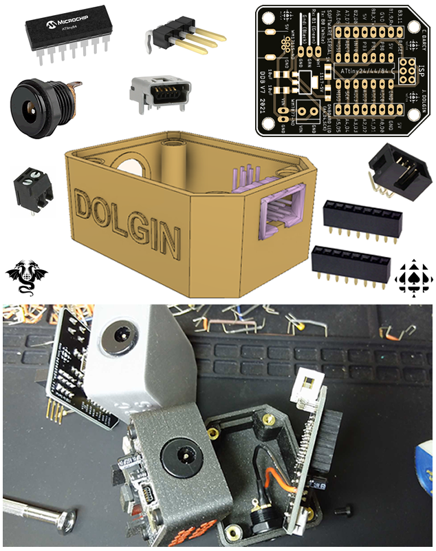
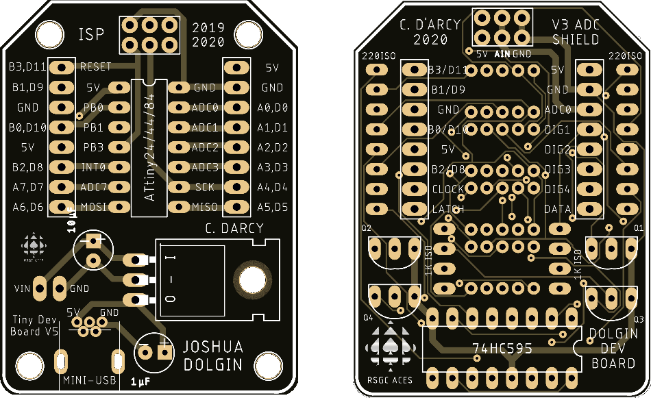
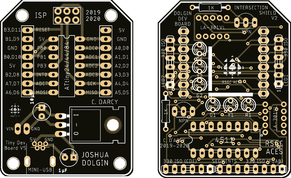
ACES are introduced to the creation of Printed Circuit Boards (PCBs) in their Grade 11 year. From the outset, they are encouraged to imagine a circuit board that would enhance ALL ACES learning experiences, not just their own. It was in the Spring of 2018, that James Corley (ACES '19, Queen's Comp. Eng. '23) designed a breakout board for AVR's ATtiny'84, perhaps feeling the UNO's ATmega328P was unnecessarily extravagant for many simpler projects. A DirtyPCB rendering of James' breakout board appears to the right and although it proved to be usable, there were a few aspects James would have modified had he revised his design and produced version 2. That never materialized as James moved on to other projects.
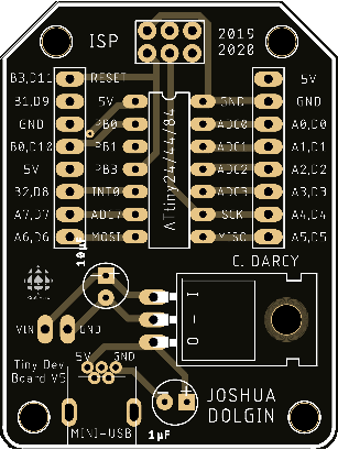
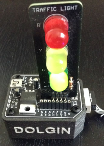
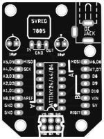 Fast forward a year later to the Spring of 2019. Grade 11 student Josh Dolgin (ACES '20, Waterloo '25), possibly inspired by the potential in what he envisioned in a tiny-based breakout board and/or in James' design, produced a more refined design that was immediately recognized for its potential in providing MCU support for small ACES' devices and for introducing Senior ACES to AVR Assembly language. Again, on its return, Josh soldered up one of his prototypes and it performed as expected. At that point Josh extended permission to have his design modified with the aim of adapting it for use in the ACES III course to introduce students to AVR (mid-level) Register and (low-level) Assembly language programming experiences.
By the time version 5 of the device arrived in the DES in September 2019, we had a platform which could be put into use for the first time in January 2020. As it turned out, the modifications were primarily about tradeoffs between power and ISP access points rather than any deficit of supporting components.
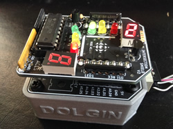
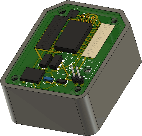 Josh's contribution to the project did not end there. His advanced design skills yielded a specially designed case to support undermounted power and ISP access to the board, thereby decluttering the access to the device from the top. The uniquecombination of the board and the custom case has justified the rebranding of this insanely useful DES asset as the Dolgin Development Platform.
EAGLE and Fusion 360 design files for this platform (.sch, .brd, and .f3d) can be downloaded for your personal use from,
https://github.com/rsgcaces/AVROptimization/tree/master/DolginDevelopmentBoard
My intent for this repository is to supplement it with your DDP Shield design files coming later this year....
1. DDP: Assembly
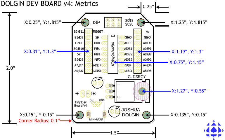
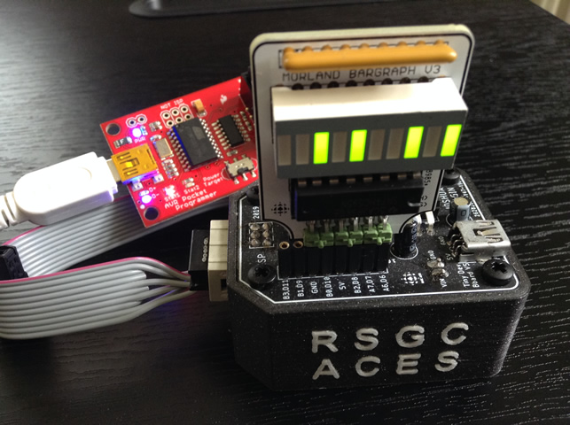
 Your first (pleasant) task is to prepare the hardware and software environments for the Dolgin Development Platform (DDP). On the hardware side assemble your DDP using the parts supplied to you. See the full Parts Table below, right.
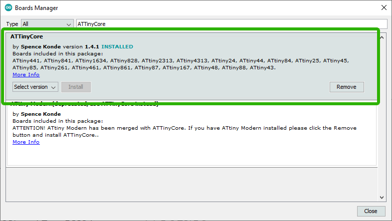
On the software side, within the Arduino IDE, under Tools > Board > Boards Manager, be sure to have installed the latest ATtinyCore library by Spence Konde. You may wish to create a DDP folder within your Work area to hold this term's software investigations. Writing similar high-level code that you have been doing for the UNO, open, modify, save as, and test the Blink sketch to confirm your DPP supports flashing an LED on any of the digital pins available. Uploading code to the DDP is accomplished through the undermounted ISP header using your Sparkfun AVR Pocket Programmer (USBTiny).
Friday's class is a work period to complete these DDP hardware and software preparations as well as allowing DER time for the first stage of the DDP. Submission is due the next day on Saturday January 11.
2. DDP: Testing
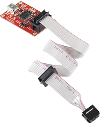 With your Dolgin Development Platform environment in place we are now ready to begin exploiting its capabilities. Whereas the Arduino platform has onboard USB to Serial support, our lean DDP relies on ISP programming. For this, you'll use your handy Sparkfun AVR Pocket Programmer, inserting the ISP cable into the under-mounted ISP connector.
Another design feature of the DDP is that once your project is functioning, you can remove the ISP connection, detach the programmer section (pictured to the right) and simply insert its power cable into the Mini B connector on top to power your creation. Very convenient (It's likely clear to you by now that the DDP's access point design decisions that you've encountered already were purposely intended to maintain low headroom on the top of the platform. Hence, you'll have unobstructed access to the ATtiny84's header pins for your future DDP Shield project).
Task.
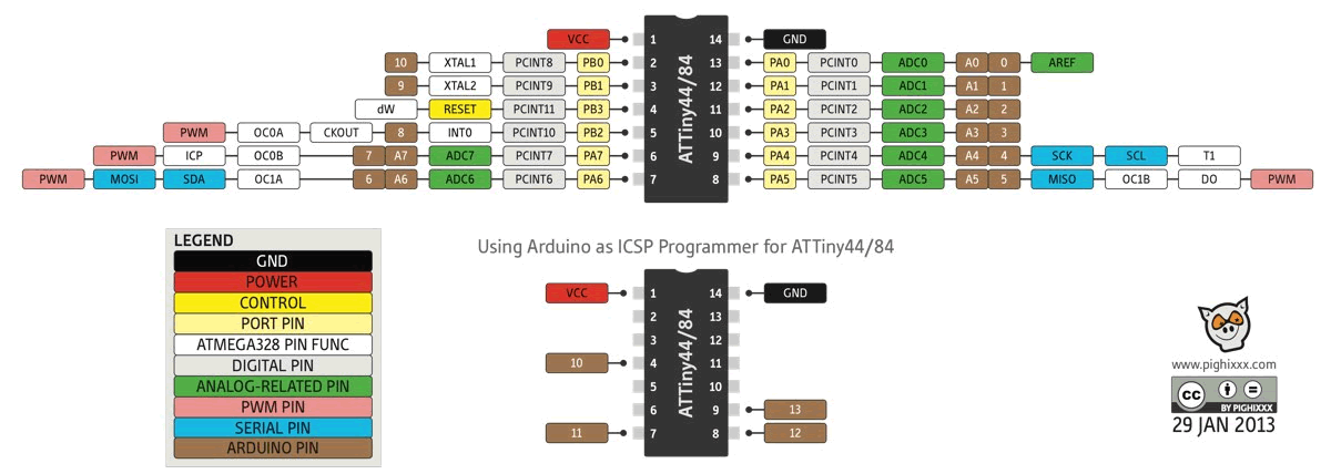
- Click on the image below and familiarize yourself with as much of the ATtiny84's pin arrangement and functionality as possible.
 Create a DDP folder within your Arduino sketch folder and condition yourself to placing all of the sketches developed for use on the platform in this folder.
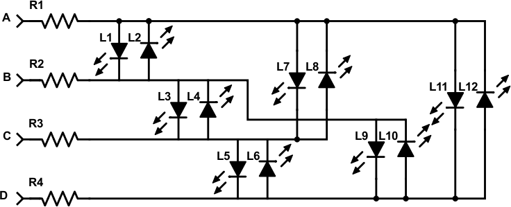
- Run through a familiar sequence of devices and high-level programming practices to get acquainted with our new environment. Provide evidence in your first DDP DER entry that you have successfully implemented the following three trials: the single LED blink sketch, the Schaffer Traffic Light, and the Morland Bargraph. For the latter, you'll note that the power supply and digital pins of the ATtiny84 have been broken out in a manner perfectly suited for this device. Be sure to highlight this in your Report. I suggest you showcase the following four Morland Bargraph capabilities,
 Simple, recognizable binary sequence or alternating pattern
 Shift out
 0xFF and demonstrate a 'breathing' bargraph by placing a signal on the 595's output enable pin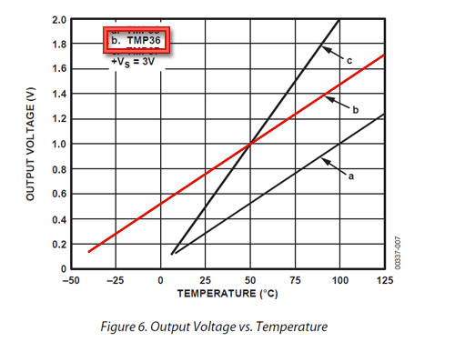
 Review Adafruit's TMP36 terrific tutorial. Now, what's great about the DDP is that without support of the Serial Monitor, we're (somewhat) blind. However, our Morland Bargraph is an output device that can tell us a great deal if we exploit it correctly. So, wise ACES will, first, familiarize themselves with the TMP36 in a more 'informative' environment. Wire the TMP36 from a breadboard to your Arduino UNO and explore its output with the help of the Serial Monitor. OK, with a better understanding of the device, insert it into a strategic location on the DDP and project the result of an analog reading of the sensor on your bargraph over an appropriate thermal range of your fingers while pinching the device. You can either present the raw readings or tailor it as VU meter with a little math. (
map() and constrain() are handy functions for this application as is bit-shifting). Some other creative and inspiring exercise of your own choosing. Look in your kit and come up with something compelling.
Finally, pack these four Morland Bargraph exercises into a single sketch with some strong code design decisions. Note, the mark you will receive will be based, in part, on how unique your code is from that of your peers.
DDP: USB to TTL Serial Cable
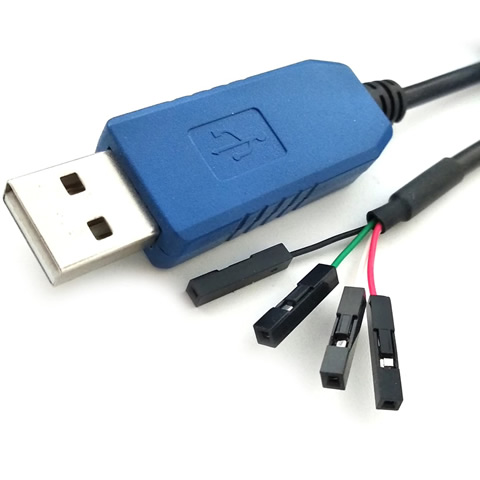
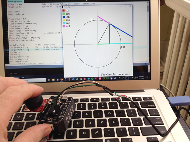
A solution to the benefit of serial streaming to the Arduino Serial Monitor and Plotter from the DDP comes in the form of a USB to TTL Serial Cable from Adafruit (below, left). The basis for this discovery comes in the form of this instructable from OldArkie in whch he describes a similar approach from the ATtiny85. The image below, right (click to enlarge) is of a dynamic application of a thumb joystick in a DDP running a sketch (SerialOutputDDP.ino) that streams the 2D coordinates to a Processing application (CircularTrigFunctions.pde) developed to introduce students to the true origin of the six trigonometric functions: The Circular Functions. USB cable connections to the DDP can be determined by looking closely at the photo. The White 5V wire is not connected.
I'll provide a demonstration in class on the resumption of classes after the March Break 2020. Both sketches are available from  DDP's GitHub repository.
| Adafruit USB-to-TTL Serial Cable #954 |
DDP Control over the Processing Circular Function Sketch |
 |
 |
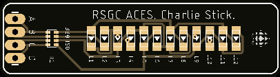
3. DDP: CharlieStick (Register-Level Coding)
 References
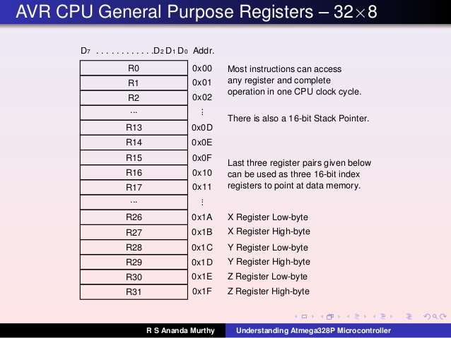
- ATmega328P Datasheet. See Section 36 starting on page 612.
- ATmega328P Include file: iom328p.h
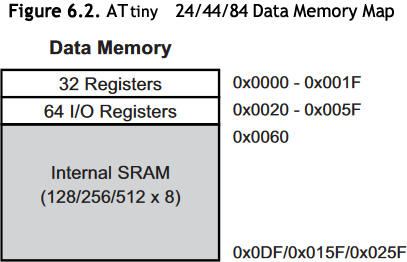
- ATtiny24/44/84 Datasheet. See Section 24 starting on page 182.
- ATtiny24/44/84 Include file: iotnx4.h
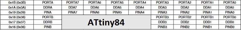
- Search for evidence within the ATtiny84's iotnx4.h file that confirms the information in the adjacent Data Memory Map graphic.
- After digesting the previous references you'll appreciate that the header file simply consists of hundreds of
#define compiler directives that provide aliases for the specific AVR MCU registers and bit-within-a-byte numbers.
- Last fall, in Project 3.2 you were asked to explore Charlieplexing and tasked with implementing our new charlieplexed SimonStick. as Project 3.2.1. As a followup task, Project 3.4.2 asks that you adapt your previous sketch by maximizing your use of Register-Level coding strategies and other
#defines from the header file to have your SimonStick function as a VU meter for the TMP36 temperature sensor.
 CharlieStick (Register-Level Coding)
Note: Both devices are expected to be implemented as DDP appliances. You'll have to think strategically for this.
Terminology
An Appliance is an ACES term for a PCB-based device that is inserted vertically into a SINGLE female header on either the UNO or the DDP. The Schaffer Traffic Light (STL), the Morland Bargraph (MB) and the CharlieStick, are three examples.
A Shield is the conventional Arduino term for a PCB-based device that spans BOTH female headers, horizontally, on the UNO. ACES have adopted this term in reference to a device that spans both headers on the DDP.
In late 2019, two DDP Shields were developed for ACES to continue to develop their MCU prototpying skills. By the end of the term, after working extensively with these two shields, every ICS4U ACE will have the opportunity to add to the inventory of our DDP Shields through the creation of their own, original, Legacy Shield for future ACES to benefit from.
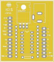
4. DDP: ADC Shield
 This Shield exploits the 10-bit Analog-to-Digital Conversion feature of the ATtiny84 (oddly enough, the DIP14 ATtiny84 offers 8 separate ADC channels as compared to the DIP28 ATmega328P's 6.)
- Download the EAGLE Files for this Shield and examine them closely. You'll likely exploit these later in the term when you design your own DDP Legacy Shield
- Q. How are the signals for the 2×3 female input header arranged?
- Q. Considering the other shield components what software technique is employed to present the reading?
 After our thorough group discussion of the design and cautions, solder the Shield carefully as some parts are irreplaceable (2mm pitch, LA-301VL).
- Review the side-by-side pairing of the DDP base (left) and the ADC Shield below (click to enlarge). The silk-screening will enable you to determine and
#define the corresponding port/pin usage. Note. When you create your own DDP Legacy Shield do not overlook the benefits of smart silk-screening to those that follow you.
- Develop and confirm your code's A/D conversions for your TMP36 (make sure you confirm the correct orientation) a trimpot, and a voltage divider made from an LDR and fixed resistor.
- Your code SHOULD,
- employ data smoothing using a history list of AT LEAST 50 readings
- inhibit leadings zeroes in the display, and,
- include the low-level shiftout function we developed in class earlier in the week
- Comment your modular code, extensively.
5. DDP: Intersection Shield
 In this Shield segment, our Schaffer Traffic Light (STL) gets a serious upgrade. Watch this clip of the simulation,
  DDP: Intersection Shield (1:08)
- Download the EAGLE Files for this Shield and review the connections thoroughly. Take as much DESIGN information into consideration as you can for your similar Legacy Shield effort later this term. Also, since this Shield is more densely populated than the ADC Shield, there was not as much room for silk screening. You'll have to dig deeper into the EAGLE files to determine the pin assignments. Too many of you did not do this sufficiently in the previous ADC Shield project and wasted time and credit as a result.
- Again, the Intersection Shield uses two, narrower-pitched, 7-segment displays (2mm pitch, LA-301VL). SOLDER THESE FIRST, using a FINE point solder tip, taking great care to avoid solder bridges, spills, and leaks.
- Develop code to match the video sequence and timing as closely as possible. Stretch your register-level coding skills as far as you can, including the use of the register-level
shiftout() function discussed previously in class.
- Comment your MODULAR, EFFICIENT, COMPACT code, extensively.
6. DDP: Legacy Shield
 ACES' tradition reflects a popular culture trope in which Master Craftsmen Make Their Own Tools. A quick review of the ACES PCB Archive supports this claim. In this latest attempt to enrich the engineering experience of the ACES that follow, you have the privilege of being the first group of Sr. ACES to develop an original set of DDP Shields.
What is unique about this PCB task is the myraid of constraints placed on the design of the PCB Shield, not the least of which are its dimensions. Furthermore, by the time ACES are ready to assemble their DDP Shield, you can assume they have SMD/T experience.
Task.
- If you have not done so already, create EAGLE projects from the .sch and .brd files available from our RSGC ACES' Dolgin Development Project repository.
- Review these designs and come up with the best idea you can to allow ACES to explore concept(s) that you found particularly compelling. The best designs are typically the simplest, least expensive, most flexible and easily adaptable to the broadest range of applications. Feel free to bounce your ideas off me before or after school.
- After settling on your idea, download and copy the Shield files (Intersection and/or ADC) that are a better fit with your plans, remove component you do not need and start designing. You only need to ensure your board outline remains identical, as do the positions of the two 1×8 headers that connect to the DDP motherboard.
- Be sure to use the ACES SMD/T EAGLE resources available from the top of our course page to expedite your results.
- By the deadline, attach five files (DER.docx, .sch, .brd, .cam, and .zip) to an email to handin under the Subject Line: DDP: Legacy Shield.
- Ideas? TTC Line 1 (Coding skill), Breadboard Shield (Prototyping), Sensor Shield (Testing), 0.96 OLED Display, ?
7. DDP: AVR Assembly Language Programming
7.1 References
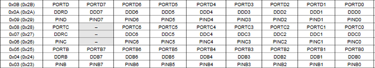
7.1.1 GPIO Port Summaries
7.1.1.1 ATtiny84
7.1.1.2 ATmega328P
7.1.2 Summary: AVR Assembly Instruction Set
7.1.3 Detailed: Online AVR Assembly Instruction Set
7.1.4 Full Manual: AVR Assembly Instruction Set
 7.2 Exercises
7.2.1 Inline (8-bit) AVR Assembly (within the Arduino IDE)
In our first few AVR assembly exercises you will explore how the AVR-gcc toolchain permits the interspersing of assembly language statements amongst Arduino C statements through the use of the asm () macro. This blog offers a primer...The following video provides a good foundation for AVR Assembly concepts in a little more detail than is required at the moment but, nevertheless, is highly instructive: Intro to Arduino Inline Assembly
7.2.1.0. The Fastest! Blink
In a previous exercise you successfully confirmed that setting a bit in an AVR Port's PIN register, toggled the corresponding bit in its PORT register, leading to the fastest way to blink an LED. In this first exercise we'll perform the same task, in assembly language.
Task.
- Insert an LED into your DDP spanning A0 and ground.
- Within an
InlineAssembly folder, create a New Project called BlinkInline.
- Within your
setup() function , add an asm volatile () macro that declares PORTA, pin 0, for output.
- Within your
loop() function, add an asm volatile () macro that writes 1 to PINA, pin 0.
- Using the builtin
delay() function add a 1 second delay between loop iterations.
7.2.1.1. (All Assembly) Delay
 A clock cycle is a tick of the MCU's oscillator. The source of these ticks typically comes from the MCU's external crystal or internal RC clock.
As you can imagine, the benchmark measure of the efficiency of any code sequence rests with determining the number of MCU clock cycles (or simply clocks) it takes to execute, not the absolute amount of time the code takes to execute. Courses in your university Comp. Eng, program will require you to explore this this so let's get a simple taste, now. Further reading: AVR-libc Benchmarks
The delay(ms) function is handy, but unproductive, as all it does is waste clock cycles. Nevertheless, exploring an 'All AVR Assembly' equivalent to the delay(ms) function is instructive for our ends. So, although the previous exercise confirmed that inline assembly and high-level C can coexist, this exercise allows you to explore replacing the high-level delay(ms) function altogether through additional assembly instructions inside our loop() function's asm volatile( ) macro. In doing so, we'll also acquaint ourselves with a few more AVR instructions.
Task.
- Review the AVR Instruction Summary I've posted online. The last column indicates the clocks for each instruction.
- Follow this link for a more comprehensive AVR Instruction Reference.
- Q: How many clock cycles does the
sbi instruction consume in execution?
 Review this handy code generator calculator for wasting AVR clock cycles offered by Bret Mulvey. (Wise ACES will right-click the page and review the Javascript source code to deepen their understanding of these important code techniques) An inspired JS enhancement was made by T. Morland, ACES' 18, (of Morland Bargraph fame) which I'll explain in class. You'll also find this utility by click the DELAY link at the top of our course page, as you'll want to exploit its value, often.
- Q: Load the AVR Delay Loop Calculator and go to the last text input box (cycles), enter the number 100, and press go. Select avr-gcc and examine the assembly code. Explain why the assembly code is correct (for this value) in terms of wasting clock cycles. Try additional multiples of 100 up to 800. Any comments? Conclusions?
- Complete the entries to generate an equivalent sequence of Assembly instructions as a replacemnt for
delay(1000). Again, choose the avr-gcc syntax for now.
- Load your
BlinkInline sketch from the previous class and remove the call to the delay(1000) function. Copy the auto-generated code from the previous step and insert it into your loop() function's asm volatile( ) macro.
- Listen closely to the additional explanations in class to have your code run as expected.
7.2.2 Standalone (8-bit) AVR Assembly Coding (within the Arduino IDE)
Reference (unnecessarily complicated but informative, nonetheless): https://rwf.co/dokuwiki/doku.php?id=smallcpus
 The Arduino IDE offers painfully few tools for the aspiring assembly language programmer to develop a skill set but it has one important thing going for it: familiarity. Make no mistake, confidence, coupled with steady productivity and reasonable success, are required to sustain interest in the challenge of low-level coding and, so far, you're making SUBSTANTIAL progress.
So, let's keep the hardware task the same (fastest blink of an LED) but strip away the cumbersome " " and \n from inline assembly to write clearer, standalone, AVR assembly code.
7.2.2.1. The Fastest! Blink
 Within a folder called
 StandaloneAssembly, create a first project called FastestBlink.- (Now, this step will seem weird...) Delete ALL comments and code from
FastestBlink.ino leaving the file completely blank. (an informative action would be to compile (verify) this empty file and read the diagnostic error messages it produces. Remember, all the code you have ever run in the Arduino IDE operates within the C driver shell main.cpp)
- So, if we hope to have any of our own code run within the Arduino IDE, we require, at the very least, both a
setup() and loop() function. We'll now provide these functions in Assembly!
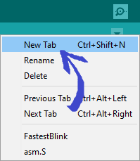
- Our standalone assembly code will be placed in a completely different file, within the project, with the extension,
.S (Note: it MUST be a capital S). Look to the top right corner of the IDE, click on the dropdown button, select New Tab and, in the text box, label the new file, asm.S. (Note: you could call it anything you want but let's keep it consistent for today)
- Now, enter the code below in the
asm.S. file. The .global assembler directive is one of many that assists the toolchain with the creation of the final executable. Functions in assembly language are simply labels. Furthermore, it should be obvious now that they terminate with a ret statement.
.global setup
setup:
	ret

.global loop
loop:
	ret
- You can now add the familiar assembly statement to the
setup function, free from the " " and \n syntax required in inline assembly. Comment appropriately.
- Additionally, add the familiar statement to your
loop function. Comment appropriately.
- For our kill function, a
.global directive is not required as this function requires only local access (ie, not visible to other files in the project that will be linked together). Return to our AVR Delay Calculator to obtain assembler code for the body of our kill function that will simply waste 1s worth of clock cycles. Comment appropriately.
- Add opening comments within your
asm.S file, upload. and admire!
- Note 1. The Auto Format feature does not apply to assembly code. You must do this by MANUALLY.
- Note 2. EVERY assembly statement deserves a meaningful comment. Get used to it.
- Note 3. Compile this code and COMPARE the amount of program storage space it requires to the standard
File>Examples>Blink sketch.
7.2.2.2. Schaffer Traffic Light
 In this second standalone AVR Assembly exercise we return to the venerable STL to continue to expand our knowledge base of instructions. Setting (or clearing) an individual bit od a PORT is handy, but typically you'll want to affect multiple bits at a time. For these purposes you'll need the
 in and out instructions.
Place your Schaffer's Traffic Light into DDP pins A2..A0 + GND.
(conveniently, the Intersection Shield works just as well for these exercises)
7.2.2.1.1 Version 1
- Within your
AssemblyStandalone folder create the project STLv1.
- Clear the
STLv1.ino file and add an STLv1.S tab.
- Insert the
.global functions setup and loop.
7.2.2.1.2 (Improved) Version 2: AVR Assembly delay(ms) Function
Rather than entering and exiting multiple asm volatile () blocks, Version 2 accomplishes the same result with a single asm volatile () block by replacing the Arduino C delay(ms) function with an assembly function that does the same thing (waste clock cycles).
- Save your successful
STLv1 project as STLv2.
- Review the Mulvey/Morland utility for determining just how many cycles to waste. Since we're exploiting the ATtiny84's internal 8 MHz RC clock, enter the parameters to generate code for a 1s delay (we'll use the avr-gcc version for this sketch).
- This auto-generated code introduces you to a few new assembly instructions (ldi, dec, brne).
- If this 1s assembly code sequence could be structured to reflect a function, it could simply be called n times to waste n seconds! This will introduce the rcall and ret assembly instructions.
- Within a single
asm volatile () code block in the setup() function, run the STL continuously for same the 3s-1s-3s delay sequence.
7.2.2.3. Morland Bargraph
 With the AVR assembly language branching and looping structures underway, we can turn to our familiar friend to strengthen our command of these skills in the orchestrated manipulation of port bits required by the high-level
 shiftout() function. Something worth recalling is that shiftout() and SPI signal waveforms are not too dissimilar.
An earlier examination a couple of months back took a mid-level register approach which we studied intently, that we can now take to an even greater depth.
By way of review, in our Meet this week, we'll review a second mid-level register approach using the AS7's ability to develop for the DPP in it's C dialect (you are encouraged to write some C code for yourself, for practice). Download and review the Word document prepared specifically for you in support of this lesson: MorlandShiftBarC.docx
You'll see by the photo, that the placement of the MB3 in the DDP span both its A and B ports which will need to be addressed in both the C code we will review, and the ASM code you will be required to develop.
Seven Segment Counting
To strengthen your skill set, I have carefully developed an integrated set of increasingly-complex projects based on the DDP and the ADC Shield especially for you; the 2019/2020 ICS4U class. It's imperative that you take the concepts that you have been taught, acquire these skills, and prove to yourself you can handle a degree of complexity.
 To start, Using the AVR Assembly knowledge gained so far, in particular our Data and Labels lesson, you are asked to present single digit counting, either on a standalone 7-segment display or, preferably, on your ADC Shield. I have prepared a video of what I expect you to develop:
Seven Segment Counting Support Video
I have broken down the necessary steps below to such a degree that anyone with even the slightest bit of motivation and interest in preparing for the challenges that lay beyond RSGC should be able to fulfill.
Task.
- Create a project called
Shiftout7Segment.
- Within the Program Flash section (
.cseg or .text), define a 10-element array of segment maps of the form (0Babcdefg0). This will require the use of the .DB or .BYTE directives.
- Declare start and end labels, before and after your array (aka. Lookup Table or LUT).
- Your code should assign the start and end labels to the 16-bit X and Y (pointer) registers as I demonstrated thoroughly last class in the Data and Labels lesson.
- Next, turn on the active 7-segment display by ensuring ground access for the display, If doing this on a single CC display, simply wire pin 3 or 8 to ground. If using the ADC Shield, the rightmost display as shown is grounded by setting
PA4 (which is connected to the base pin of its low-side transistor). These assignments can be determined from theADC Shield's silk-screening.
- Your code will undertake a continuous loop with the Z register pointing to the same starting LUT address as the X register and advancing by 1 (autoincrement) until it reaches the Y address. With each iteration, the value from the LUT (pointed to by Z) is shifted out to PORTA using the MSBFIRST direction.
- Insert a 1 second delay between digit presentations.
- The result is a continuous display of the digits from 0-9, repeatedly, as shown in the video.
Be prepared for Monday in the event you get randomized for a Show&Tell.
PoV on the ADC Shield
 This project is a consolidation of previously undertaken AVR skills, investigations, and projects. The first DDP Shield you worked with, the ADC Shield, has a set of four, fully-resisted, 7-segment displays, accessible through the use of the onboard 595 shift register, using a Persistence of Vision (PoV) scheme. The PoV is enabled as the ATtiny84's port pins
 PA1..PA4 are tied to the respective base pins of the four, low-side NPNs that provide ground access to each of the CC displays, in turn.
Task.
- Create the project:
PoVontheADC.
- Through the use of labels and the
.DB (.BYTE) directive, your code should define an 10-element array of segment constants within the .cseg (.text) section, defining the state of the LEDs in the order 0Babcdefgx.
- Hard code a value between 00 and 99 into Program Flash with the
.db directive (or .byte if in the Arduino) to be displayed on the ADC Shield using your shiftout function from a previous project by the same name.
- Shifting out should be undertaken with
MSBFIRST if the segments are defined as indicated in the previous step.
- The correct
DATA, LATCH, and CLOCK equates can be found in a recent post to the ICS4U Conference.
- As stated, the PoV strategy is accomplished by repeatedly signaling the base pins of the transistors to pull the CC displays to ground. The base pins are attached to
PA1 through PA4.
- Document and format your code to a standard that reflects the handouts I've prepared for you.
- Bonus: For the motivated amongst you, I encourage you to take this project up a level. I could have asked for a 16-element array of segment constants (0-F), asked you to hard code a value between 0000 and FFFF, and requested a 4 digit PoV display.
Attach JUST two files ONLY: DER.docx and either main.asm (or PoVontheADC.S if you develop within the Arduino IDE) by the deadline.
 Pseudocode for this Algorithm...
- Define a 10-element segment Lookup Table (LUT) in Flash (same as previous task)
- Assign to
number the two-digit value (eg. 99) to be displayed
- Reserve two bytes of storage in SRAM for the as-yet-to-be-determined tens and units digits of
number
- Define a register
count to hold the tens digit. Initialize it to 0
- Assign to
Z the address of number
- Load
r16 with Z (number) with the lpm instruction
- Subtract 10 from
r16
- If the result is less than 0, (the tens digits has been determined:
count) advance to Step 10 (brmi)
- Increment
count and go back to Step 7
- Store
count in the first of two SRAM storage bytes reserved in Step 3 (sts)
- Add 10 to
r16 (this is the units digit) and store to the second reserved byte in SRAM (sts)
The two digits have been separated, stored in RAM bytes, and ready for PoV display...
- Load
Z with the starting address of the LUT
- Load
r16 with the units digits from SRAM (lds)
- Add
r16 to ZL to have it point to the correct segment map in the LUT
- Load
n with the value pointed to by Z (lpm)
- Turn off the tens display (DIG3) (
cbi) (remember, we need to reduce ghosting)
- Call your
shiftout function
- Turn on the units display (DIG4) (
sbi)
- Pause for a PoV-suitable interval (see Lesson 69 on our course page)
- Load
Z with the starting address of the LUT
- Load
r16 with the tens digits from SRAM (lds)
- Add
r16 to ZL to have it point to the correct segment map in the LUT
- Load
n with the value pointed to by Z (lpm)
- Turn off the units digit (DIG4) (
cbi) (remember, we need to reduce ghosting)
- Call your
shiftout function
- Turn on the tens display (DIG3) (
sbi)
- Pause for a PoV-suitable interval (see Lesson 69 on our course page)
- Go back to Step 12
7.2.2.4. Morland Bargraph Array Presentation
To be developed...
7.2.2.5. CharlieStick
To be developed...
7.2.2.6. CharlieArray
To be developed...
To be developed...
7.3 Standalone Assembly (Atmel Studio 7)
Yikes! :)