| 2022-2023 ICS3U-E Engineering Tasks |
![]() Project 2.6. R-2R Digital to Analog Conversion (DAC)
Project 2.6. R-2R Digital to Analog Conversion (DAC)
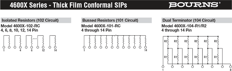
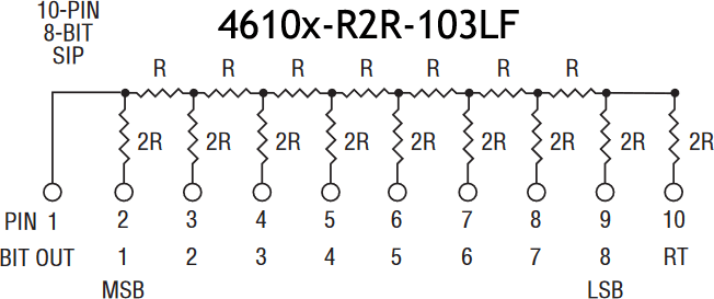 to include the R-2R design (right). You were supplied with such a device in your Session 6 loot bag, the datasheet for which can be found here.
This project asks that you wire up a 8-bit DAC using slide switches and your R-2R ladder to yield an analog output. A DMM or even Analog Voltmeter will be used to confirm the output. It might be a good time to dust of that 12V supply.
Our final few classes complements our earlier look at wired communication strategies (Serial, SPI, and I2C) by introducing two wireless protocols: Infrared (IR) and Radio Frequency (RF). You are invited to explore Bluetooth on your own should you feel drawn to it. The second part of Project 2.5 requires you to demontrate your competency with one of these wireless strategies in developing a remote control system oover your mechanical prototype developed in the first part of Project 2.5.
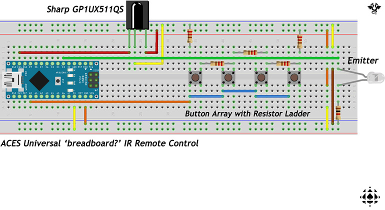
Following our brief look at a possible prototype for a universal remote control you may wish to extend the concept by adding additional codes to control your mechanical device.
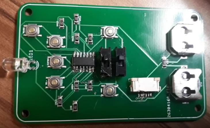
Fola Folarin (ACES '20, Waterloo '25) chose to develop a surface mount version of an IR remote control for his Medium ISP in Grade 12 (pictured, right). Here is Fola's video that accompanied his DER submission: ![]() The DominatIR 2.0
The DominatIR 2.0
 2. Two-Way nRF24L01 Communication
In your possession are a pair of nRF24L01 transceivers. In class you were introduced to one-way communication between two MCUs, supported by the use of these devices to transmit a byte from a base UNO to a receiver UNO.
In this project you have the opportunity to solidify these skills by extending the sample application to support an interesting two-way communication. For example, earlier this year you undertook an exchange between a UNO and a Nano that employed wired serial communication when you complete the ASK,UNO project below. This project offers you the chance to modify that project by employing the pair of nRF24L01 transceivers you have.
Feel free to replace the Nano with a second UNO if that's more convenient and borrow a second breakout board from a peer if necessary.
![]() Project 2.5a Mechanical (This is a 2-part Project - Think Mini-ISP :)
Project 2.5a Mechanical (This is a 2-part Project - Think Mini-ISP :)
 This project provides each of you with an opportunity to pull from all (four) ACES Domains: Software, Hardware, Design, and Communication. With a final term ISP off the table and plenty of time to meet the two remaining deadlines, you have a glorious chance to achieve something of real value that could be a wonderful addition to your university application next fall. These projects have made the difference for many graduatiing ACES in the past by opening the doors of opportunity.
Almost without exception one of your first memories is that of a mechanical/motorized toy you received as a gift and played with endlessly. With luck, you may still have it somewhere, either in your room or a basement toy box. This project gives you the opportunity to revisit some of the mechanical magic you were enthralled with over a decade ago and may consider pursuing in your post-ACES years as a Mechanical/Mechatronics undergraduate.
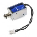
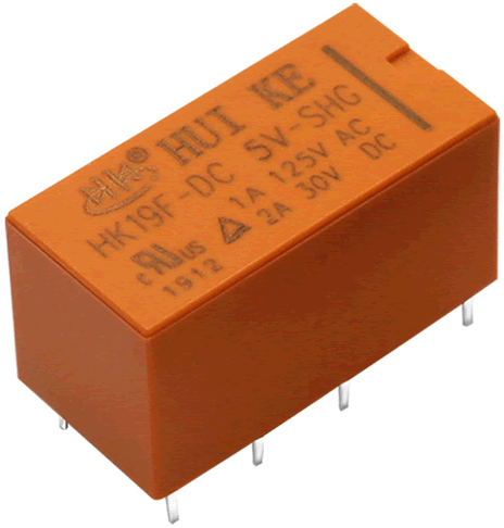
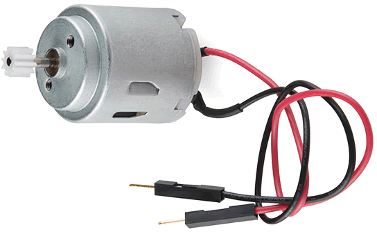
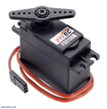
Our instructional focus explored the mechanics of five common electromechanical devices (solenoid, relay, DC hobby, servo, and stepper motors) shown below. In the first stage of this this 2-part project, you are asked to identify one (or more) of particular interest to you and develop an compelling prototype that exposes both its (no load) capabilities and your command of the many related hardware and software concepts you have become familiar with in this course. These include power supply considerations, MCU control, monitoring, measuring, and display options, and finally some simple design aspects (PCBs, acrylic and/or 3D printing mounting and encasement alternatives). For the truly inspired, a sixth option is offered to you. The common denominator of these electromechanical devices are copper coils that generate a magnetic field. If electrical engineering is still a possible future objective, consider winding your own coil and undertaking research, analysis, appllcation, and remote control over your device.
| Solenoid | Relay | DC Hobby | Servo | Stepper |
 |
 |
 |
 |
.png) |
The emphasis of this project is on creativity, originality and making the best use of the available resources in front you (components and time) (the only caution I will issue is that if your ISP or previous ACES project involved one of the three motors above, and you a wish to exploit it again, you are expected to take it to entirely new level)
As a starting point for your project considerations, you may wish to review the videos on our course page submitted by the 2020/2021 ICS3U class that were tasked, specifically, with monitoring the speed of their DC Hobby Motor. Here's a link to their project description. Interestingly, their efforts were undertaken with the first month of the COVID pandemic. Browsing a decade's worth of previous ICS3U course pages will bring you face-to-face with dozens more project videos from Grade 11 ACES that have gone before you.
Finally, one of the reasons I require ACES to document their achievements in text and media (and painstakingly archive their work) is to have them available for inspiration for current ACES to use a springboard for their own accomplishments. Josh Dolgin's Bi-wheeled Rover and Jasper Schaffer's Rubiks' Cube Solver (both undertaken as Grade 12 ISPs) are pinnacles of high-school project achievements you can exploit to open the doors of your admission to University Engineering programs, this time next year.
![]() ,
, ![]() or
or ![]()
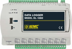
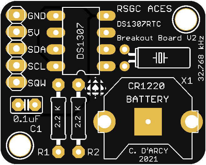
![]() Project 2.4 I2C Data Logger
Project 2.4 I2C Data Logger
Combine the proliferation of time-dependent sensing devices with the increased frequency of power disruptions, and you make a strong case for robust embedded systems to feature built-in logging functionality. Commercial Data Loggers such the one pictured (below, right) are readily available but can impose significant cost and form requirements. ACES can engineer better.
Expectations
 You are asked to create a device that exploits I2C communication in the logging of the ambient temperature of an environment for a single 24 h period, as frequently as your hardware storage capacity will permit.
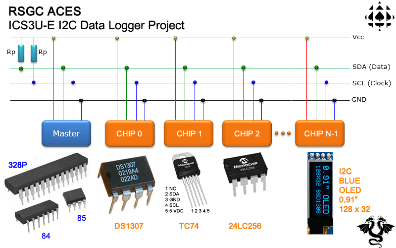
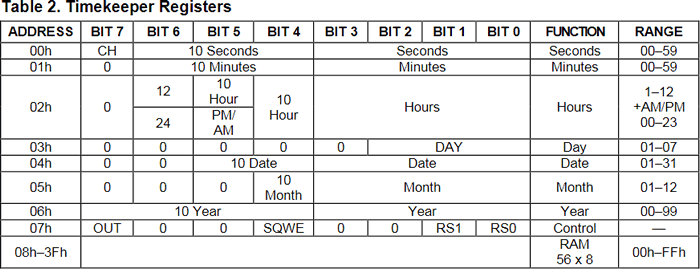
Your review of the DS1307RTC datasheet indicated that the IC has 56 Bytes of on-board non-volatile memory (NV RAM) spanning addresses 0x08 through 0x3F. This memory is a viable candidate for data logger storage location (Silver only) or an embedded system in the event of either a system or power failure.
As I've indicated in the past I believe the path to the best version of one's self MUST include choice. ISPs are the primary vehicle ACES use to follow an engineering path you're drawn to. Within THIS project there are similar paths you can take in pursuit of its primary and secondary objectives. On the spectrum below assess where your current situation lies (available time, interest, motivation, passions, etc...).
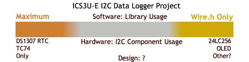
GD assisted me with designing your project choices/options. On Tuesday January 31 you will be asked to commit to one.
This will allow each of you to gain a measure of benefit while fitting with your time, motivation, and interest levels.
| PROJECT CHOICES/OPTIONS | BRONZE | SiLVER | GOLD |
|---|---|---|---|
| MAXIMUM MARK | 9.0 | 9.5 | 10.2 |
| COMMITMENT | JM, SL | WA, BB, LD, DF, JMi ARC, RS, JS, CT, BW |
JC, GD, VJ, LM, AS |
| MCU | mega328P | mega328P, tiny84, tiny85 | Your Choice (Arduino IDE) |
| Number of I2C Devices | 2 | 3 | 4 or more |
| Wire.h | Yes | Yes | Yes |
| Third-Party I2C Library Use | Tes | Optional | No |
| EEPROM | mega328P | MCU, DS1307, or 24LC256 | 24LC256 |
| Arduino EEPROM.h Library | Yes | Optional | No |
| GRAPHIC Data Display | Serial Plotter | Any | Processing or Excel or Graphic OLED |
| Board | Breadboard | Any | Soldered |
| Encasement | No | Optional | Yes |
| HID Controls | No | Optional | Yes |
Requirements Consistent with your Project Choice
 Develop an embedded system that schedules and records temperature readings for a 24 h period to EEPROM (NVRAM)
| RSGC ACES' DS1307 BoB V2 (2021) | RSGC ACES' DS1307 BoB V3 (2022) |
 |
 |
![]() Project 2.? Numeric Coprocessor.
Project 2.? Numeric Coprocessor.
The brain of an embedded system is the primary MCU. A (CO)processor is (was) a secondary processor specially designed to perform efficient floating point calculations. To be developed...

![]()
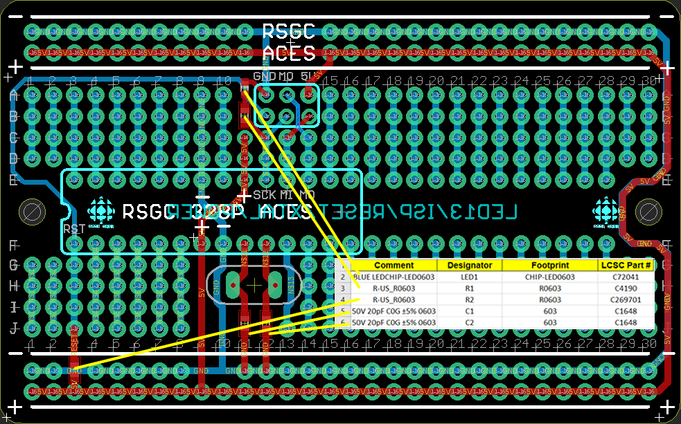
![]() Project 2.3c Perma-Proto ATmega328P with PCB. Most (all?) ACES projects combine required elements with creative latitude for students to demonstrate competency in both areas. It is your teacher's belief that your careers will demand this of you. This project is representative of this hybrid pairing.
Project 2.3c Perma-Proto ATmega328P with PCB. Most (all?) ACES projects combine required elements with creative latitude for students to demonstrate competency in both areas. It is your teacher's belief that your careers will demand this of you. This project is representative of this hybrid pairing.
The goal of the embedded system designer is to engineer a real time, in-system programmable (ISP) and functioning MCU-based device, housed in a physical and electronically-stable case. This project gives you your first attempt at creating such a device (and sets your design ideas in motion for our custom PCB and CAD design journey in the weeks ahead)
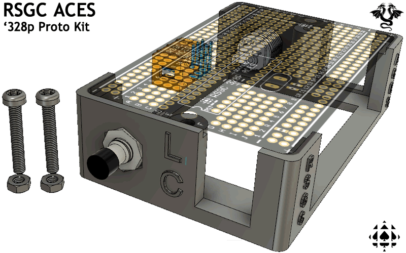 The ULTIMATE GOAL of this project is to create a mounted, standalone, sensor-based, In-System Programmable (ISP) (MCU reprogrammable without removing it) device driven by the same MCU at the core of the Arduino, AVR's ATmega328p that was secured to a 3D Printed ACES Stand in Stage 2 of this project series.
Task
Now, with your EAGLE PCB skills at the ready, your task is to design and engineer one or more PCBs that integrate into your functioning perma-proto platform. You are encourged to think of your existing platform as a motherboard control system and what you design in EAGLE can be aptly referred to daughterboard plugins. Designing your daughterboards with male headers that plug into female headers you can add to the motherboard gives you maximum flexibility for testing back on the breadboard version of this project and allows you to go back to JLC or other CAM house for improved versions of your PCB devices.
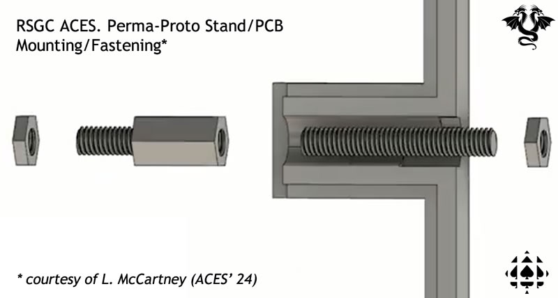 Also keep in mind the underside of the ACES Perma-Proto Stand was designed to be open for easy access to the underside of Perma-Proto ATmega328p half-size PCB. There are a lot of flexible options here for your creativity.
I'm sure you'll think of a more optimal layout. Just remember, those 30 columns are precious, so make the best use of them as your design skills will permit. Finally, I am of the opinion that the most successful projects are the ones in which the designer/engineer has a clear image in his or her head and a reasonably accurate drawing on paper. This is one reason I ask ACES to include a hand-drawn sketch with their ISP proposals. So, consider engineering this project in reverse by reading all three project stage descriptions and prototyping backwards.
Submit your full report by the deadline. Enjoy the world of possibilities this project opens up.
![]()
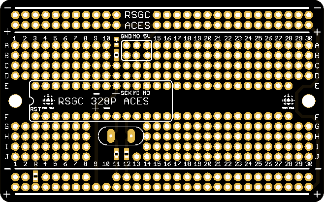
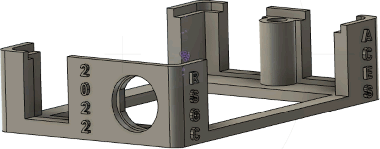
![]() Project 2.3b Perma-Proto ATmega328P
Project 2.3b Perma-Proto ATmega328P
| ACES' ATmega328P Perma-Proto Half-sized PCB | |
|---|---|
| Rendered View | RSGC ACES 1/2 Perma-Proto Kit |
 |
 |
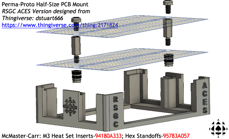
| Supplemental (Basic) Parts List for 2.4 | |
|---|---|
| # | Description |
| 1 | RSGC ACES Perma-Proto 1/2 Sized PCB |
| 1 | 28-Pin Kinked IC Socket |
| 1 | 2 × 3 Shrouded ISP Header (Wurth) |
| Supplemental (Conditional) Parts List for 2.4 | |
| # | Description |
| 1 | RSGC ACES 1/2 Size Perma Proto Mount |
| 2 | M3 5 mm Nylon Screws |
| 1 | Coloured PBNO with Leads |
| * | Heat Shrink Tubing |
| ACES' ATmega328P Perma-Proto Half-sized Kit (PCB and Mount) | |
|---|---|
| RSGC ACES 1/2 Perma-Proto Kit System | Functioning System |
|
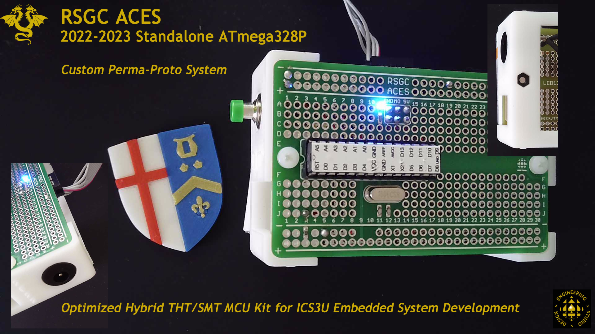 |
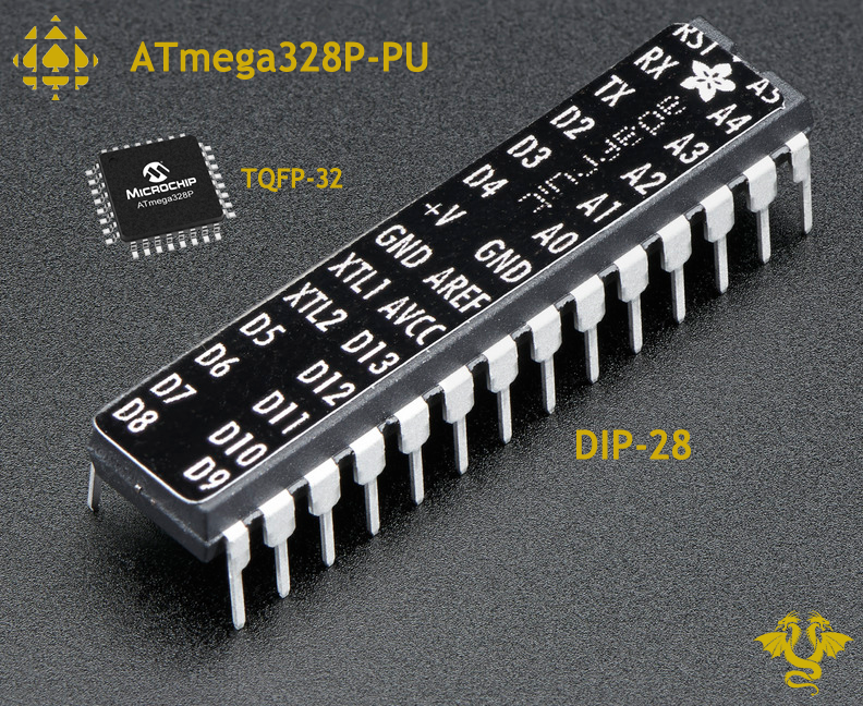
![]() Project 2.3a Breadboard ATmega328P. With a term's worth of introductory awareness of the Arduino's capabilities, it is time to strip the MCU from the convenience of well-appointed development boards (UNO, Nano, etc.). By placing the ATmega328P DIP28 IC into an empty breadboard and bringing it to life, you come to appreciate the minimal set of supporting components required to support embedded systems of your own future designs. Familiarity with minimally-design systems helps to reduce costs and maintenance. Furthermore, this project is the ideal segue to designing your own custom PCBs for your ISPs.
Project 2.3a Breadboard ATmega328P. With a term's worth of introductory awareness of the Arduino's capabilities, it is time to strip the MCU from the convenience of well-appointed development boards (UNO, Nano, etc.). By placing the ATmega328P DIP28 IC into an empty breadboard and bringing it to life, you come to appreciate the minimal set of supporting components required to support embedded systems of your own future designs. Familiarity with minimally-design systems helps to reduce costs and maintenance. Furthermore, this project is the ideal segue to designing your own custom PCBs for your ISPs.
An underlying objective in this new, three-part project (culminating in late February) is to expose you to inseparable interconnection between Design and Engineering. The first stage begins as you have become accustomed, with a breadboard prototype of a standalone MCU circuit. The second stage, the control system, gives your circuit a sense of permanence using components custom designed for ACES in EAGLE and Fusion 360. Engaging these components is intended to provide you with ideas and design possibilities for your own ISPs that you will be introduced to later in this course. The third stage is where a custom PCB of your own design integrates into your stage two control platform for what can be decribed loosely as an Embedded System.
Read this Standalone ATmega328P Primer
Read this (Previous Year's) Comprehensive Backgrounder on a similar Project
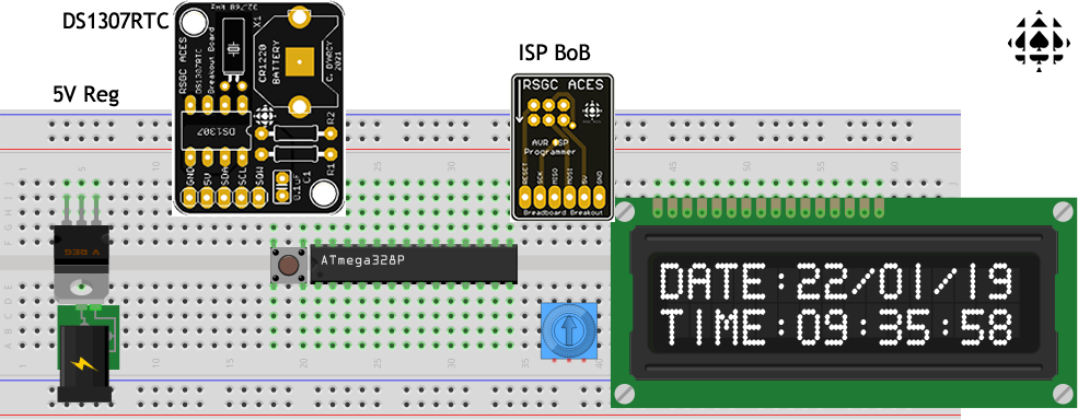
![]() Project 2.? A Breadboard RTC.
Project 2.? A Breadboard RTC. ![]() for 2022/2023. One of the advantages (and privileges) of running a program of our own design like the RSGC ACES program is that I get to continually adjust my curriculum to meet the immediate needs of my students and many dynamic challenges beyond our control. After the previous Persistence of Vision project, you all needed to make adjustments to the full project development cycle, particularly the final reporting phase. I was thrilled with the way you responded to our post-project discussions last week and I want to acknowledge and reward your efforts. So, here's how I intend to do this.
for 2022/2023. One of the advantages (and privileges) of running a program of our own design like the RSGC ACES program is that I get to continually adjust my curriculum to meet the immediate needs of my students and many dynamic challenges beyond our control. After the previous Persistence of Vision project, you all needed to make adjustments to the full project development cycle, particularly the final reporting phase. I was thrilled with the way you responded to our post-project discussions last week and I want to acknowledge and reward your efforts. So, here's how I intend to do this.
Our class-time last week and this week are invested in exploiting your PoV experience in the development of a breadboard-based, real-time clock system. Not only does this pursuit introduce you to an important (wired) communication protocol (Inter-Integrated Communication or I2C) and a number of other essential techniques and skills, but the process provides a useful model for your own first personal ISP undertaking over the next two months.
Task.
 Continue to follow along closely with our in-class development of a breadboard clock prototype, noting and documenting (media) the numerous stages and concepts that are brought together to produce your working.
This (Friday and) Saturday, assemble our mutual experience into your own unique DER presentation while adhering to hundreds of details and expectations provided in the previous months in our program. To capture the highest credit possible you will pay close attention to both the individual and group feedback comments that have been provided to you. To this end, you are NOT to simply wear out a path to my desk this week seeking multiple assurances that you are doing things to the letter. Doing so will only reduce your eventual credit. You are all capable of completing the reporting task ON YOUR OWN or with the OCCASIONAL query to a TA.
Make the most of this opportunity.
![]() Project 2.2 Persistence of Vision
Project 2.2 Persistence of Vision
(Reference: AVR Foundations: pp. 35-38). It's strange to think that our eyes perceive much of the LED lighting around us to be uniformly ON, when they are actually OFF as much as half the time (maybe this is one of the reasons LED lighting is so cost-effective?). The next time you're in the DES, point your phone's camera at the digital clock and observe the interference bands generated by clock's display alternation and your camera's periodic scan rate.
 |
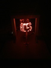 |
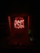
Perhaps the most remarkable ACES PoV creation was engineered by K. Fiset-Algarvio (ACES '19, Guelph Mech. '23) in his amazing Grade 11 ISP:![]() The Persistence of Vision Globe. Above are two images extracted from his DER. Be sure to watch his detailed video.
The Persistence of Vision Globe. Above are two images extracted from his DER. Be sure to watch his detailed video.
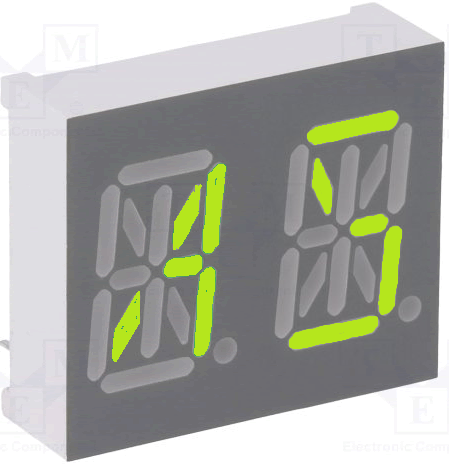
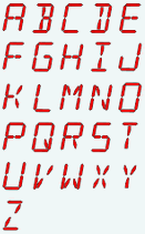
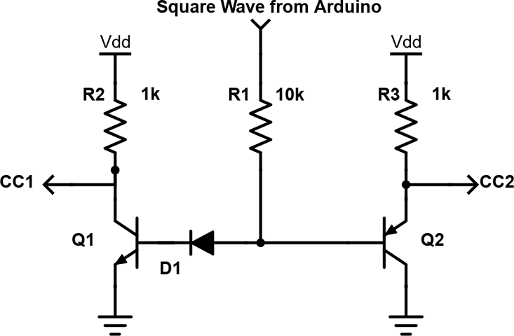
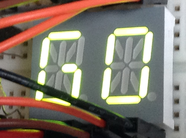
You have been given a dual 14-Segment Dual CC Alphanumeric Display. An image of the device appears below, left, in which I have coloured a few segments to simulate a 'possible' depiction of the two-letter word AS. Here's the link to its datasheet so you can familiarize yourself with its pin layout. Given its 14 segments, this component can be driven by two SN74HC595 shift registers* and a pair of transistors (one NPN and one PNP) under control of a SINGLE square wave (bottom, right), in a Persistence of Vision scheme.
*Although the ATmega328p has enough pins to complete this task without using shift registers, you are required to do so, for practice.
 |
 |
 |
BASIC Task. (Adapted for 2020-2021)
For the ambitious, consider the following any or all of the following. If you implement any enhancement add a section on you DER entitled Enhancement and document your creative extension(s).
ENHANCED Task.
Advice (trust Mr. D's experience)
 This is a CHALLENGING project. Do NOT doubt yourself, you are all talented enough to complete it. Success follows those who simply devise a SMART plan and have the DISCIPLINE to execute it.
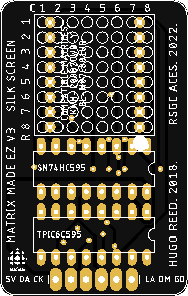
![]() Project 2.3. Persistence of Vision. For his PCB project in Grade 11, Hugo Reed (ACES '19, Queen's '23) imagined, designed, and developed a handy PCB that future Grade 11s could exploit to hone their LED matrix animation skills. We're going to incorporate Hugo's terrific little device into a creative implementation.
Project 2.3. Persistence of Vision. For his PCB project in Grade 11, Hugo Reed (ACES '19, Queen's '23) imagined, designed, and developed a handy PCB that future Grade 11s could exploit to hone their LED matrix animation skills. We're going to incorporate Hugo's terrific little device into a creative implementation.
Parts List for Hugo's MatrixMadeEZ PCB (all can be found in your toolkit),
The header will enable your device to be mounted vertically in your breadboard, driven by your official (or breadboard) Arduino, or even an ATtiny84 or ATtiny85. Note. this is NOT an appliance for the UNO as there is no 5V access on the digital pin side.
Basic Task
 Using the exposure gained through hardware and Persistence of Vision software techniques introduced in class you are asked to imagine and implement your own creative animation on your MatrixMadeEZ V3 device.
 Enhanced Task: Etch-A-Sketch
 Using your (loaner) Thumb Joystick as the 2D input device...TBD.
![]()
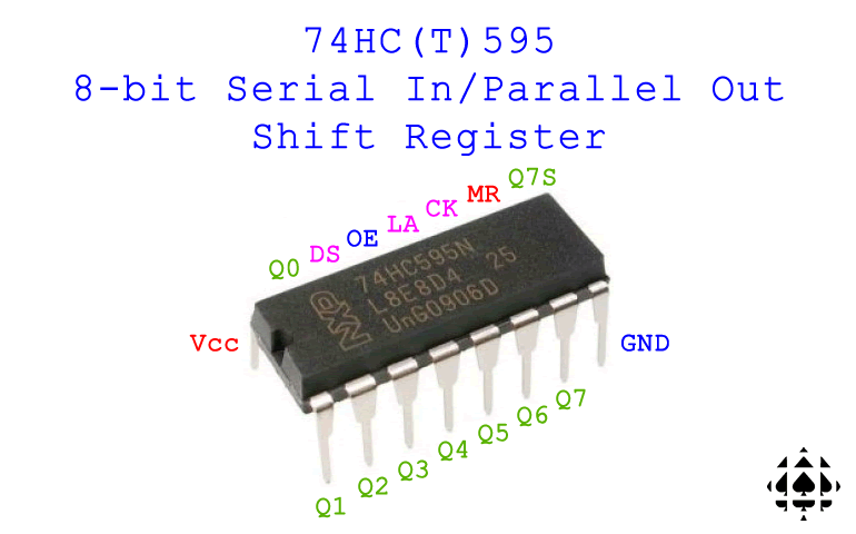
![]() Project 2.2 74HC595 Shift Registers
Project 2.2 74HC595 Shift Registers
The NCC offers (relatively) hassle-free hardware and software access to the I/O pins of the Nano (ATmega328P). Your teacher believes a month-long investment in the device addresses student background H&S deficiencies of the past and, in turn, pays handsome dividends in the projects to come. Two tradeoffs of the past few weeks, however, are that your wiring/prototyping skills may have oxidized and, more importantly, in practical terms, tying up 16 MCU pins to simply address 16 LEDs, is massive overkill. This project addresses both shortcomings and offers you an opportunity to showcase your newly-acquired H&S skills.
As stated, the NCC's 1 : 1 PIN : LED pairing is an expensive design strategy. The NCC device maps 16 pins to 16 LEDs. Fortunately, there are numerous strategies for optimizing this ratio, the most popular of which is to extend the number of MCU pins through the use of a device known as a Shift Register. We'll use the 74HC595 Serial In Parallel Out Shift Register IC. Through this strategy, you will 'design better' in that only 3 pins will be required to address 16 LEDs. As you will also come to realize, the 3 : 16 PIN : LED ratio can be extended to 3 : n when n is (somewhat) unlimited!
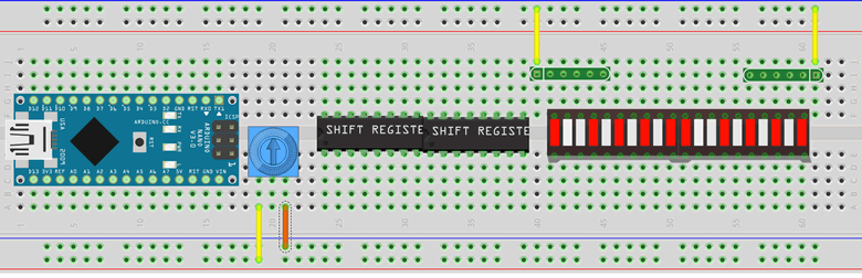
The (COMMON) hardware layout for this project appears in the Fritzing diagram below. With the exception of the two resistor networks that will be provided to you, all of the parts shown are already in your possession.
Task.
 The dual purpose of this project is to demonstrate your H&S skills in addressing 16 LEDs that result in a creative optical display of your choosing and to prioritize prototype build quality.
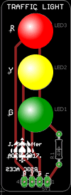 Since many of you will be pursuing your driver's license in the near future, the focus of this first project is the careful soldering and QUALITY programming of a standard traffic light. Jasper Schaffer (Fraser's older brother) (ACES '18, Queen's '22) was in his ICS3U year, when he designed the handy little PCB pictured to the right that has been the recent tradition of the first project of the ICS3U of the ICS3U year. For the assembly aspect of this project you will solder one each of a green, yellow, and red 10mm LED and a four-pin right-angle header from your toolkit onto the Schaffer Traffic Light PCB you have been provided with. Take care as there are NO replacement parts. The right-angled male header pins allow your device to be inserted directly into adjacent female port pins on your Arduino (eliminating the need to use a breadboard and hookup wires). ACES refer to these kinds of PCBs as appliances. Be sure to document your soldering of the device through media acquisition from your phone that you can include in your Report. For the testing aspect, you will include media as well as a well-planned Arduino sketch (program) modified but based on our discussions and models in class. The fully documented sketch should cycle through the LEDs continuously with the green and red remaining on for four times the duration of the yellow (amber) LED.
In your Report, you are include the Purpose, Reference, Procedure, Code, Media, and Reflection subsections in Heading 2 style. A full Parts Table, with background shading consistent with your previous ICS2O colour theme and width of 3" and should appear right-aligned within the Procedure section. Finally, ensure that no content is allowed to spill into any of the four page margins. For this first submission, I will review the requirements and techniques for inserting syntax-highlighted Arduino C Code into your Report in class this week.
Attach your DER.docx to an email (from GMail) to ACESHandin@rsgc.on.ca with the Subject: Traffic Light, by the deadline.
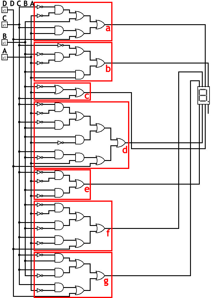
The CD4510 and CD4511 ICs are a terrific matched pair. The CD4511 BCD to Decimal 7-Segment Decoder is an integral component in last year's Counting Circuit project. The four inputs lines DCBA (8-4-2-1) were put through the internal combinational circuit that yielded seven outputs (abcdefg) that drove the common cathode 7-segment numeric display. A representation of the internal circuitry appears to the right (a similar schematic can be found in your DC Circuits Workbook).
On the other hand, for some reason the industry has not seen fit to provide a similar match for the CD4516. Why is there no CD4517 IC? For the inputs 10102 to 11112 the CD4511 simply blanks all segment outputs. In this task you will address this deficiency in software emulation.
An additional combinational logic circuit for the hexadecimal digits A through F (10102-11112) has been prepared for you. Click to view the circuits and manually confirm, by hand, one or more segments for a given set of inputs.
Task.
Finally, for the curious, the process by which combinational circuits producing a set of outputs can be determined for a given set of inputs involves a process developed in our Grade 12 ICS4U-E course.
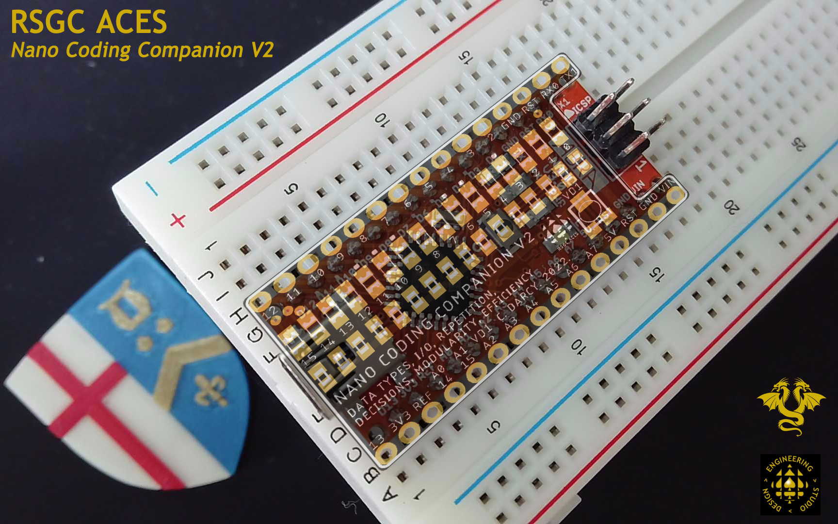 Having completed the numerous examples prepared for you, you are asked to create an interesting demonstration of your own that exploits the capabilities of the Nano Coding Companion.
Your example should make maximum use of the onboard assets of the NCC. Analog pins A3 through A5 are available for your application however the Arduino C library does not support A6 and A7 as these pins are not present on the DIP-28 package (UNO) of the ATmega328P.
A premium result will reserved for software that reflects both the great coding concepts discussed in class and hardware efficiency.
For those that complete our full ACES program, next to your Secondary School Graduation Diploma,
your DER will be your most important high school document.
The two of them will open the doors to your careers.
Take great pride in your craftsmanship of your DER; you'll be pleased you did.
![]() Project 2.1 The 555 Time Machine
Project 2.1 The 555 Time Machine
First, make the following edits to your DER,
![]() Premise
Premise
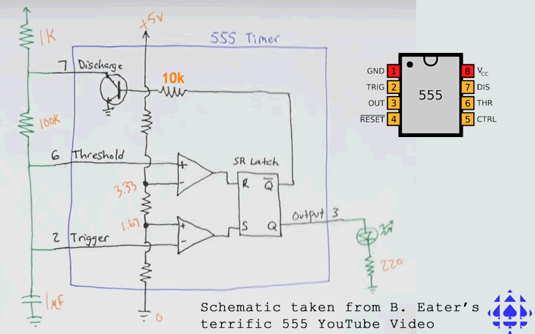
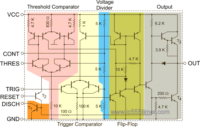 For those students anticipating an undergraduate program in computer or electrical engineering I can think of no better first project to begin your second course within our ACES program this one. Digital (and Analog) signals are the backbone of both of these branches of engineering and the venerable 555 Timer IC that has underpinned countless interesting projects for over 40 years provides numerous insights when explored in detail. As a black box, this IC can provide square wave (clock) output, in either monostable or astable mode, with varying frequency determined by the use of one (or two) program resistors and a capacitor.
Falstad provides marvelous animations that introduce you to, not only to the 555 output, but the internal architecture required to produce it. It is this simulation that you are asked to replicate in this first project of your Grade 11 year.
References and Research
Task.
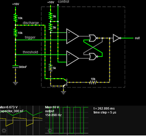 As I said from the top, this circuit is an excellent bridge from Grade 10 concepts and an important one to prototype at least once in your life. The insights it offers should inspire future ISP project choices.
 Infrared Remote Control