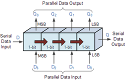
 1. Hardware. A shift register is a device typically used to expand the number of pins of a microcontroller. The most common design by far is based on the 74HC595 architecture. Using (as few as) three pins of the MCU (coloured) you are able to control 8 (or more) data lines (QA..QH). In addition to the three pins that control shifting, two other pins (Output Enable and Master Reset) provide additional (Active Low) control over the state of the 8-stage internal register set and output latches.
The IC accepts bits serially and presents them on output pins in parallel.
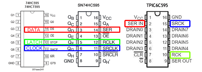
Two sets of naming conventions for pins tend to confuse those new to the IC. The image below tries to address this issue.
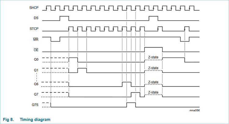
2. Waveform Details. The digital orchestration of serial input bit stream is summarized in a waveform/timing diagram. A more detailed explanation of the mechanics of Serial to Parallel Shifting-Out with the 74HC595 can be found by following the link to the Arduino tutorial. Let's attempt to decipher the timing diagram, extracted from the 74HC595 datasheet,
As you are well aware, the immediate benefit of the Arduino shiftOut function is to hide the details of the digital dance allowing the high-level programmer to concentrate on more macro concepts. However, hiding details always comes at a cost; if not performance then, at the least, in understanding. Our goal is to solidify our lower-level coding skills through direct handling of the digital signals on the three control pins, thereby bringing you closer to the AVR and IC hardware. This brings all sorts of future dividends.
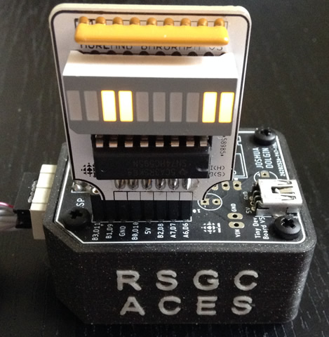
3. Prototyping Platform. The breakout arrangement of the DDP's pins was designed specifically for Morland Bargraph support. Insert the MB appliance into the DDP's feature-suitable position (supply and PWM).
 4. Register-Level shiftout. With the waveforms of the 74HC595 understood, we can now tackle the low-level port pin manipulation of the builtin
 shiftOut() function ourselves. Remember, our goal is to enlighten, not suggest this is the preferred alternative in all cases.
- Open a new sketch and save as
RegisterLevelShiftOut.
- After completing your opening documentation, create a set of four
#define directives that match the hardware/port pin pairings. The one for the rightmost one in the photo would be #define ENABLE 1<<PA6
- Now, replace the default
loop() body with the code below,
noting what you think it should accomplish,
uint8_t dir = 0xFF;
void loop() {
  for (uint8_t i = 0; i < 8; i++) {
    shiftout(dir, 1 << i);
    delay(100);
  }
  dir = ~dir;
}
- The function syntax we're going to use simplifies the conventional
shiftOut header function. We'll use a purely lowercase shiftout to avoid compiler conflict. Also, since we're designing for the DDP purposes only, we'll reduce our function's parameters to two (hard-coding the required data and clock port pins),
// LSBFIRST:0 MSBFIRST:1
void shiftout(uint8_t order, uint8_t value)
Complete the body of the function, maximizing the hard-coding of the port manipulation using your #defines.
- Questions worth considering: Where is the power coming from to drive the LEDs? Does it come directly from the MCU or does it come from the 595's output pins? What are the maximum voltage and current capabilities in either case?
Not surprisingly it's an important point that was answered pretty well on this forum...