
 Your comprehensive CHUMP journey has prepared you for the second half of your ICS4U experience: the deepest possible drilling into the hardware and software of modern microcontroller technology. The carefully designed sequence of register-level coding exercises below, exploiting familiar ACES' optical devices, is the final preparation for the final push in the Spring: Pure Assembly Language Programming of the AVR ATtiny84 on the Dolgin Development Platform (DDP).
Although these C coding exercises can be considered high-level, they call for a deeper understanding of the underlying architecture of the AVR family of MCUs. For now, this is the familiar ATmega328P, the MCU of choice for the UNO, Nano and other Arduino development boards. I often refer to this coding as mid-level, as it lies in-between high-level C (that hides much of the functionality and potential optimization) and low-level Assembly language (that you've had a brief introduction to in your 7 CHUMP instrucitons). The magic behind functions such as pinMode(), digitalWrite(), digitalRead(), and shiftOut() for example, are exposed and rewritten, in some cases, more efficiently. Direct port bit manipulation of the MCUs' General Purpose Input/Output (GPIO) Registers are called for to achieve improved performance. Conveniently, your CHUMP experience has given you the necessary insights that were lacking at the end of Grade 11 to guide these next steps.
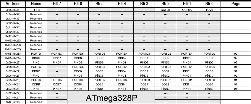
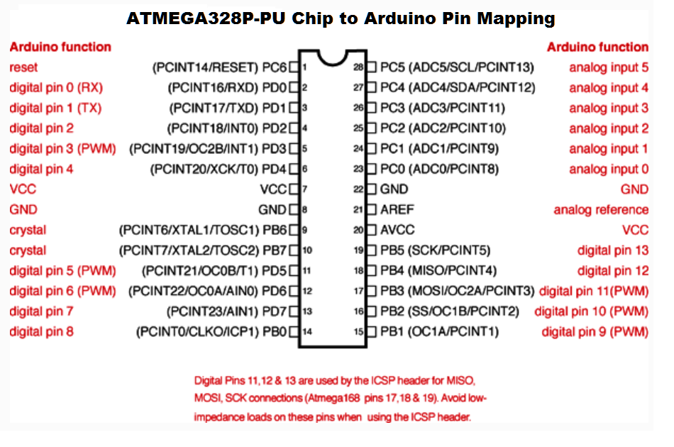
ATmega328P GPIO Register Reference
Register-Level Exercises
You may wish to create a folder entitled RegisterLevelCoding or something along those lines, to house this unique set of sketches I am asking you to develop.
 A. Bits 'n Bytes.
References
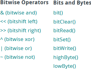
The Arduino Language Reference web page includes links to resources in support of bit manipulation.
 Two of these categories include the Bitwise Binary Operators and convenient Bitwise Functions that employ these and other operators to facilitate binary manipulation (aka bit-banging). It serves our immediate purposes with respect to knowledge and skill to code the bodies of these bitwise functions to produce the same result, ourselves.
Task.
- Create a project called BitsandBytes and drop in this shell.
- Go to our course page and insert the auto-#include header file, io328p.h that #defines the 328p's register addresses.
- Open the BitsandBytes project and review the contents of the two tabs.
- Finally, with the convenience of the Serial Monitor confirmation, employ a UNO (or Nano) in the completion of the bodies of each of the 7 functions in the list, above right, in a more efficient manner than simply calling the function.
 B. General Purpose Input/Output (GPIO) Tasks.
Note. It's not how many lines of code that matters, it's often how few.
With with the awareness that the AVR's GPIO registers are accessible by name to your Arduino C sketches, develop the most efficient register-level statements you can to achieve each of the following tasks on your UNO or Nano. The employment of register-level coding strategies precludes the use of high-level statements such as pinMode(), digitalRead(), or digitalWrite(), etc.
- Note 1. The (m-n) in front of some tasks suggests the minimum number of statements required in the setup() and loop() functions, respectively, to meet their requirements.
- Note 2. Think deeply, as the task may not be as simple as the first thought you have :)
Tasks
- (1-2) Blink the onboard LED with a frequency of 1 Hz.
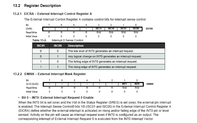
 Curious? See §13.2.2...
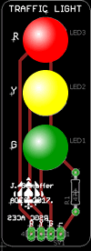
 (2-2) Place a bicolor LED in pins 4 and 5 and alternate flashing red and green, in a complete cycle every second.
- (1-4) Place your Schaffer Traffic Light into your UNO such that the R-Y-G pins are driven by pins 11-12-13, respectively. Develop register-level code that sequences the LEDs, continously, with a duration of 1s per LED.
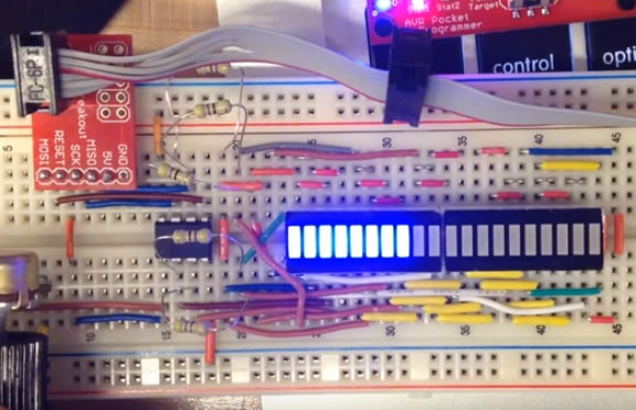
- (1-1) Add the components to a breadboard as shown below. In the first of a sequence of tasks, you are to use your Sparkfun AVR programmer, wire up all but the 595 in such a way that allows a two-statement sketch entitled, SwitchLEDEcho.ino to echo the least signficant 6 switch settings onto a bargraph.
 A Closer (Register-Level) Look at the shiftOut() Function. Click on the animated timing diagram of the shiftOut() function and study the digital signal forms, carefully. Since the orchestrated Clock, Data, and Latch forms are very similar to other protocols such as SPI and I2C, it is well worth the effort today to become familiar with their behaviour.
Task.
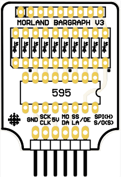
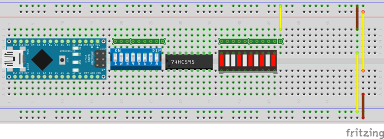
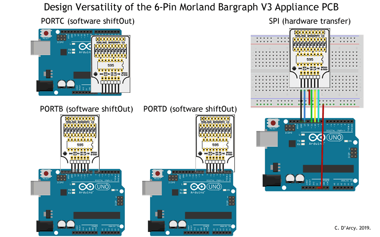
- Place your Morland Bargraph in PORTB as shown in this image.
- Develop the sketch, RLShiftOut in which you develop your own register-level shiftOut() function that uses the same four parameters as the familiar high-level shiftOut() function to echo the input from the switches onto the bargraph. For class consistency, assign the AVR pins 12, 10, and 9 as your Clock, Data, and Latch pins.
- (0-3) Binary Switches to ASCII. Make a minimum of hardware and software modifications to your breadboard prototype to permit input of the binary values of the uppercase ASCII letters [65,90] on the DIP switches and have the sketch output the equivalent characters, continuously, on your Serial Monitor.
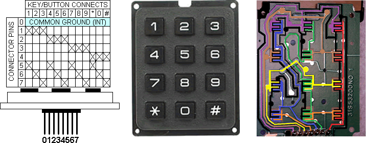
- 12-Key Telephone Keypad. An application perfectly suited to register-level coding is the monitoring of the ubiquitous 12-key telephone keypad. So many online examples suggest an intricate scanning strategy through third-party libraries. ACES say, "Balderdash!". The 8-pin header fits ideally into PORTD of the UNO or PORTA of the ATtiny84 and can be decoded with trivial ease as the 2020/2021 ACES were required to develop in their Keypad-Matrix Echo Project. Watch this video support and give it a try yourself.
- Charlieplexed ATtiny85 20-LED VU Meter. A vivid demonstration of our AVR optimization objective can be seen in the video linked to the image, below left. For this design 5 tri-state digital pins of the ATtiny85 are used to support a 20-LED VU meter using a charlieplexing strategy.
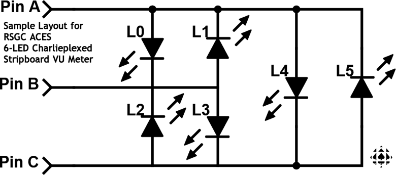
 DIY Charlieplexed 6-LED Stripboard VU Meter. The layout for a simple 6-LED stripboard VU meter that supports a charlieplex strategy appears above, right. In this exercise you are asked solder one together using the components you have been provided with in this arrangment, with L0 starting from the bottom. Three of your AVR's tri-stated I/O pins can drive this display with pins 9-11 working well if you ever intend to apply PWM the LEDs. Obtain ADC readings mapped appropriately to project onto your device.
-
 CharlieStick Dot/Bargraph. Here's an interesting challenge for your nascent register-level coding skills.
Task.
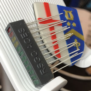
- Insert your RSGC ACES' CharlieStick, Trimpot, and Slide Switch into your UNO as shown in the photo to the right.
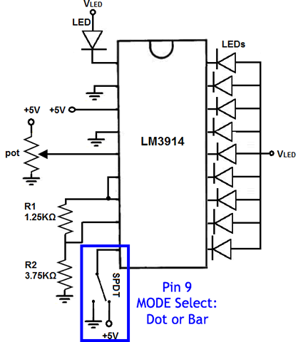
- Create a project entitled CharlieStick in which an ADC reading from your Trimpot is mapped and displayed on your 12-LED CharlieStick. The Slide Switch allows the user to request the MODE (either DOT:0 or BAR:1) in much the same manner as Pin 9 of the LM3914 Dot/Bar Display Driver.
- Charlieplex Bargraph
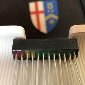
 for 2022/2023. Over the 22/23 Christmas holidays S. Appleyard and J. Rogan answered the call to design an encasement for an ACES 12-LED Charlieplexed bargragh to support an interesting Register-Level coding project we have in mind. Within two days an initial order to JLCPCB was placed for 15 units and the result was terrific. The photos below shown the first unit curing after the LEDs were epoxied in. Click to enlarge.
To be developed...
 |
 |
AVR Optimization: Create a Custom Library (Mega328P.h)
 You've employed a number of libraries over the past year or so, from the Arduino Core libraries (transparently included in every project) to third party libraries (through the explicit use of the #include directive) that hide the functionality of complex devices and tasks through convenient object instantiation and subsequent member function calls. Well, it's time to establish and exploit your own custom library. For the first attempt, you'll pack useful ATmega328P resources (constants, data structures, functions, etc.) of your own design and selection. You'll gain some familiarity with the process from completing the directed exercises below. In doing so, future projects can reuse and enhance this code to yield the desired outcomes in less time, and with improved confidence.
 Task 1. Separation of Code. First, let's consider some code that is generic enough to be reusable in future projects and confirm that it can exist in a separate file.
- Open the previous project, CharlieStick, and save it as CustomLibrary.
- Click on the Down Arrow icon in the top right corner under the Serial Monitor icon, and select New Tab.
- Enter Mega328P.h in the text box and press OK.
- Cut the identified resuable resources out of CustomLibrary, click on the new tab, and paste them into your Mega328P.h file.
- Return to the CustomLibrary tab and, just under the opening comments, add the directive, #include "Mega328P.h". Be sure to use the double quotes which reference a header file within the same project.
- Compile (Verify) to confirm all your code remains reachable, despite being split into separate files.
- Upload and confirm everything is functioning as before.

 Task 2. Centralized Access to Common Code. Now, we should place your library (the Mega328P.h file) in a folder that is accessible to all future projects.
- Close the Arduino IDE.
- Use the Finder to locate your personal Arduino sketch folder. Within this folder you have a libraries folder. This is where the Arduino IDE's Library Manager expects to find third-party libraries you have previously downloaded and installed.
- Within this libraries folder, create a new folder called, Mega328P.
- Find your CustomLibrary project folder, remove the Mega328P.h file and paste it in the newly created libraries\Mega328P project folder.
- Now, reopen the Arduino IDE, and the CustomLibrary project. Notice the tab with the Mega328P.h file is no longer there.
- Place your cursor on a new line, just after your opening comments.
- Open the Include Library feature within the Sketch menu, find the Mega328P library, and select OK. You'll notice the directive, #include <Mega328P> has been inserted into your sketch. Notice the angle brackets (instead of the double quotes as before) to indicate the library is NOT within the same project.
- Upload the code. It should be good and you can now do the same for future projects.
- As you develop new features and functions you may wish to add these resources to your Mega328P.h library file.
- ACES are committed to efficiency, accuracy, and high productivity. This world needs engineers that bring all three and custom libraries promote this goal.
Task 3. Syntax Highlighting: keywords.txt. Syntax highlightig is a useful feature that enhances code development. The key to ensuring the personal assets of our custom libraries are supported by the Arduino IDE's conventional syntax highligting scheme is a separate text file called keywords.txt.
- The official Ardiono documentation for the formatting of library keywords can be found here.
- Close the Arduino IDE.
- Download and save this keywords.txt file to your libraries\Mega328P folder.
- Open the keywords.txt file and edit it to reflect the syntax highligting apprporpiate for the use of your assets.
- Save the file.
- Open your CustomLibrary project and confirm the syntax highlighting is functioning as designed.
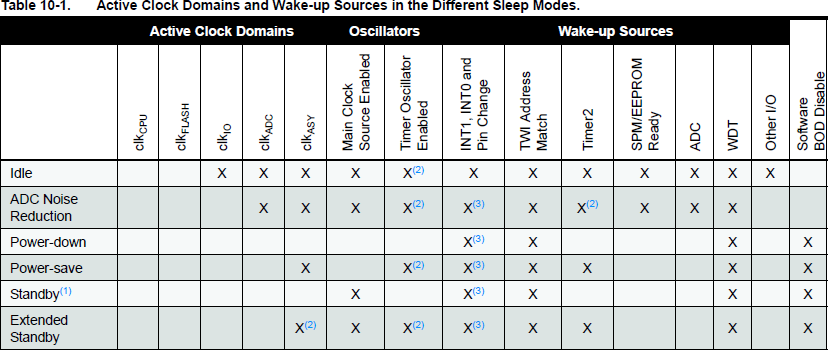
AVR Optimization: Register-Level Interrupt Coding of the ATmega328P
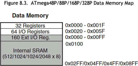
With bit-level coding of the ATmega328P's Digital IO registers (0x0020-0x005F) under your belt, it's time to excavate the next level of SRAM Addresses.
Review the ATmega328P's SRAM Register File one more time.
Here's a question for you. Based solely on the undefined (grayed out) addresses of the 328P's digital IO ports, what ports might you expect to find if you examined the ATmega2560's Register File?
Interrupts: The  to Software Optimization
Our ACES program places a high premium on productivity. Since organization and efficiency drive productivity, it is necessary to dig deeper into the architecture of the AVR microcontroller to familiarize ourselves with its capabilities in support of our code strategies and structures.
It's pretty obvious that watching your phone constantly for incoming text messages is not a productive use of your time. Likewise, standing at your front door waiting for that Amazon delivery is also a colossal waste of time. Finally, you could probably bring in the green bins from the curb rather than watching and waiting for the kettle to boil up your next cup of tea. The good news is that most of these 'Events' come with associated 'Alerts'. Today's microntrollers are no different and the AVR family is no exception. For example, the analogRead() function initiates an analog-to-digital conversion process that takes time. To the human this takes virtually no time at all but, to the MCU, these are precious clock cycles that could be used to perform a parallel task while the conversion is waiting to complete. So, wouldn't it be terrific to simply launch an analog-to-digital conversion, then do something else and wait to be alerted (ie. interrupted) that the conversion is complete and ready for reading? This sounds highly productive. The AVR line of MCUs has a builtin architecture for alerting or interrupting your code when it finishes certain tasks. We need to exploit this.
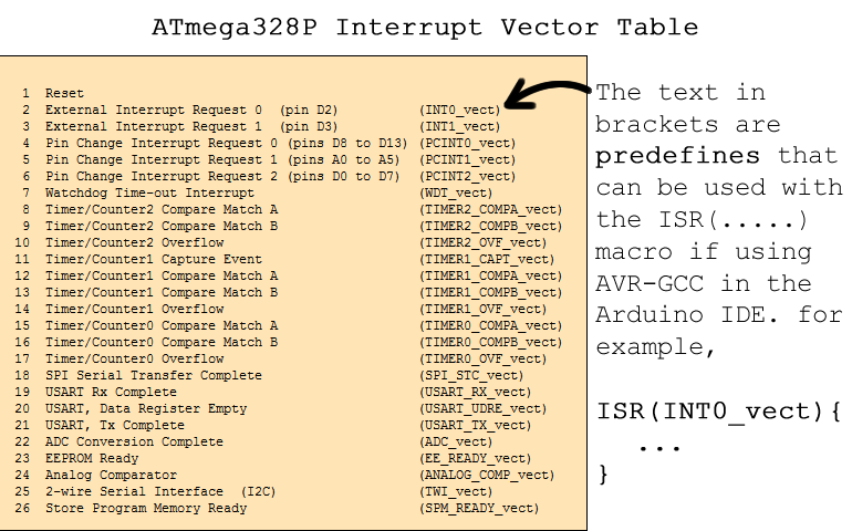 The most efficient software for the embedded developer is typically none at all. This may sound flippant but if the hardware platform your developing on has native circuitry for a given task, there is (likely) no software routine that will perform more efficiently. Review the ATmega328P's Interrupt Vector Table (IVT) to the right.
This table suggests there are as many as 26 different sources of events on the ATmega328P that have the ability to complete the following sequence,
- Automatically interrupt whatever your code is doing at that instant
- Preserve the current 'state' of your program in its entirety
- Transfer control to another section of your code ( remember CHUMP's Program Counter? )
- Execute whatever instructions you have coded as a 'response'
- When the response code is finished, automatically return you to the instruction you were executing the moment the interrupt occurred
- Restore the saved state of your code
- Allow you to continue on as before
The order in which these Interrupts are listed carries with it additional meaning. Implied in this order is a sense of priority. By being #1, a hard (or soft) Reset has the highest prioritiy and takes precedence over any other task your MCU is performing, resets the Program Counter to 0, and code starts from the beginning again. We'll start our formal implementation of Interrupt coding with the Reset Interrupt.
Interrupt #1. Reset
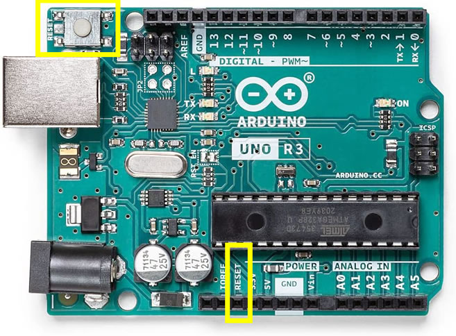 You are familiar with the effect of pressing the Reset button on the UNO or Nano, however further optimization is accessible through a deeper understanding of the subtleties the various Reset sources of AVR MCUs. These sources can be detected and subsequently impact how your code chooses to restart.
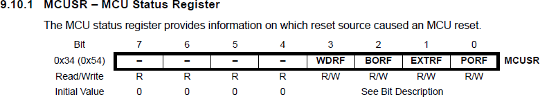
Chapter 11 of the ATmega328P datasheet introduces the concept of System Control and, in particular, the Reset Function. The MCU offers four hardware Reset triggers that include: Power On, External, BrownOut, and Watchdog. At the end of this chapter, there is a description of the Registers that can be inspected and manipulated. For our purposes, we'll limit ourselves to a simple distinction between the Power On and External Reset triggers. Page 54 of the ATmega328P datasheet presents a detailed discussion of the MCUSR Register, (see: ATmega328P Register Summary) in which the source of a Reset can be identified through the use of flags (bits).
Task.
- Span a bicolor LED across digital pins 8 and 9 of your UNO such that the green anode is in pin 8.
- Create the project ResetInterrupt328P and replace the default sketch with this one: ResetInterrupt328P.ino
- Review the fully functional code and note the (unsuccessful) attempt to identify the source of the System Reset: MCUSR's WDRF, BORF, PORF and EXTRF flags
- Upload the code and confirm the UNO lights the green LED. Which of the four Reset sources do you think this is an example of ?
- Launch the Serial Monitor and note that the green LED Lights. Which of the four Reset sources do you think this is an example of ?
- Temporarily disconnect the UNO from your laptop and then plug it back in. The green LED lights. Which of the four Reset sources do you think this is an example of ?
 Press the UNO's onboard Reset button and confirm the green LED lights. Which of the four Reset sources do you think this is an example of ?
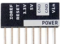
- Grab a breadboard and wire a momentary button to the UNO's female Reset header with a 10 kΩ pullup resistor as the default state. Pressing the button should place a ground into the Reset pin.
- Press your button to confirm a System Reset. Which of the four Reset sources do you think this is an example of ?
Interrupt #2 and #3. External Interrupt Requests 0 and 1 (INT0 and INT1)
From your previous year's experience you are aware that MCUs have digital pins that can be configured to respond to changing voltage levels presented by external behaviour. By way of example, the ATtiny84 has ONE such pin, the ATmega328P has TWO, and the ATmega2560 has SIX!
The two on the ATmega328P are referred to as INT0 and INT1 (digital pins 2 and 3 respectively). As can be seen from the IVT (below, left), each has a separate vector address and immediately follow the System Reset Interrupt in order of priority. An excerpt from Chapter 13 of the ATmega328P datasheet appears below right. Configured correctly, the ATmega328P can sense and respond to four voltage level behaviours presented on the INT0 and INT 1 pins.
Task.
- For this exercise you are asked to assemble a prototype similar to the one shown below. The goal is to enable the user to increase or decrease the digit displayed on the 7-Segment device through the use of FALLING edges triggered by button presses and presented on INT0 and INT1.
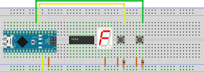
 Feel free to incorporate your 4511 BCD decoder for a presentation of decimal digits (0-9), or wire the segments independently and present hexadecimal digits (0-F) through a segment LUT.
- You may wish to debounce your button inputs for a better user experience.
- Create the project ExternalInterrupt7Segment and drop in this shell: ExternalInterrupt7Segment.ino
- On a System Reset the display should show 5 initially.
- Configure the INT0 and INT1 Interrupts to have the display increase and decrease the digits displayed respectively. TIP. Since External Interrupts are commonly implemented, you may wish to add meaningul #defines in your Mega328P.h library, designed as ORed flags for LOW, LOGICAL, FALLING and RISING.
Interrupt #4, #5, and #6. Pin Change Interrupt Requests 0, 1, and 2
 for 2022. 20/21 ICS4U ACES were the first class to be introduced to the ACES Rotary Encoder. A few short months later A. Goldman and S. Atkinson used their familiarity with the device to support their
  Clue Capturer prototype for their ECE190 course at Waterloo. Their achievement is the inspiration behind this project segment of your journey.
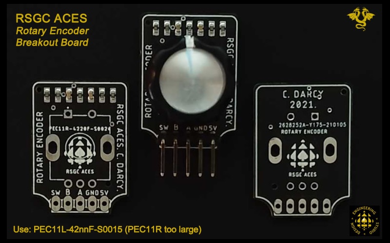
Your Bourns PEC11L-4215F-S0015 Rotary Encoder offers three sources for useful interrupts. These are A, B, and SW. Given that the ATmega328P only provides two external interrupts, we look beyond INT0 and INT1.
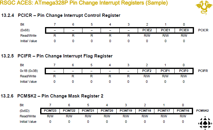
In reading Chapter 13 of the ATmega328P datasheet you discover that interrupts can be triggered on ANY digital IO pin in the event that a logical level change has been detected in hardware. A little bit of software detective work is required to determine which pin was triggered as the 24 pins (PCINT0..PCTIN23) are organized into three separate banks defined by the respective Ports. Pins on PortB are mapped to PCINT0..7, pins on PortC are mapped to PCINT8..15, and pins on PortD are mapped to PCINT16..23.
A sample of the applicable Pin Change Interrupt registers of the ATmega328P appears below.
Task.
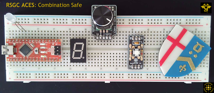
 Create the project CombinationSafe.
- You are to duplicate much of the functionality of the Goldman-Atkinson Clue Capturer prototype. A bicolor LED indicator replaces the servo with green indicating a correctly-entered combination. If so, hold the green for three seconds before retunring to red and starting again.
- Your code will update the 7-segment display digit appropriately with rollover (clockwise rotation adds 1; counterclockwise rotation subtracts 1).
- A SWitch press on te rotary encoder extends the three-digit combination sequence by the active digit.
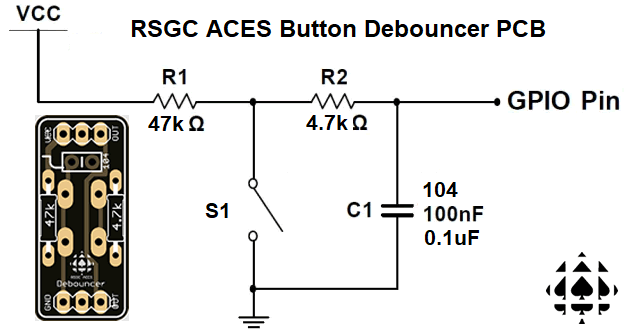
- An ACES Debouncer V2 button press resets the combination sequence.
Interrupt #7. Watchdog Time-Out Interrupt (with and without a System Reset)
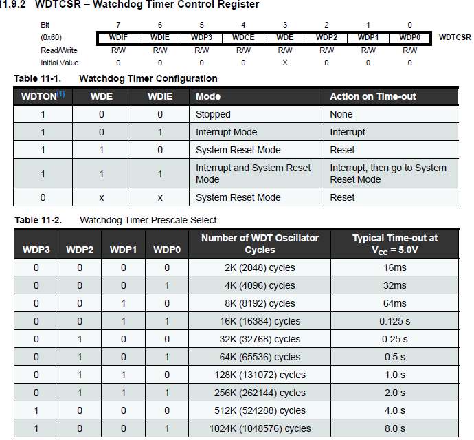
 The watchdog timer (WDT) is an MCU subsystem that can be configured to perform scheduled functionality. From the ATmega328P datasheet, 'The watchdog timer is clocked from an on-chip oscillator which runs at 128kHz. By controlling the watchdog timer prescaler, the watchdog reset interval can be adjusted as shown in Table 11-2 on page 55."
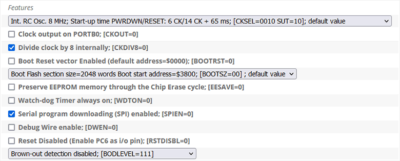
The WDTON fuse determines whether the WDT subsystem is enabled or not (see AVR FUSE Calculator). The default setting has it enabled (WDTON=0). As with any MCU susbsystem, should it not be required, advanced applications may wish to disable the feature in order to conserve power.
WDT Tasks. (Three Variations)
From Table 11-1 to the right it can be seen that there are FIVE courses of action that that can be taken following the end of an elapsed WatchDog Timer interval. We'll start with a simple Interrupt.
 Watchdog Time-out Interrupt Only (no System Reset). For starters, you'll configure the WDT to generate an interrupt at specific intervals of time based on an internal counter clocked to the WDT's internal oscillator.
- Create a new project entitled WDT328P and drop in these two files: WDT328P.ino and prescalers328WDT.h.
- Open the WDT328P project.
- Click on the prescalers328WDT.h tab and review the contents. Consider copying these constants to your personal Mega328P.h library now or simply add an #include directive to prescalers328WDT.h in your WDT328P driver to access these ORed flag constants.
- Using the embedded comments as a guide, complete the configuration of the WDT in your WDT328P driver.
- Launch and confirm.
- How could a 5-minute interval between LED state transitions be configured with the WDT?
 Watchdog Time-out Interrupt with System Reset. You may recall from the earlier Interrupt #1. Reset that there are FOUR triggers for an ATmega328P System Reset as reflected through flags in the MCUSR register, one of which is a WatchDog Timeout Reset Flag (WDRF). Note: Despite my best attempts to have the Arduino sketch identify and display the source of the Reset, it appears that too much code is executed in the avr-gcc toolchain before our code gets to read the MCUSR. IF you find way, let me know!
As alternative to the runaway code context above, it is not difficult to imagine a remotely-situated, solar-powered, MCU-based sensor device that collects (and possibly transmits) data to a centralized location. Understandably, optimum use of power would contribute to its viability and sustainability. This segment provides some insights into how some aspects of such a prototype could be implemented to conserve power between readings. One video I encourage you to watch is Kevin Darrah's Low Power Arduino! Deep Sleep Tutorial. This presentation contains applicable material for this investigation.
 Power-Down Sleep. With the WDT tool confirmed as a scheduler, if there's nothing to be done between interrupts the MCU's power demands should be reduced to a minimal level after configuring the WDT interrupt to wake up the MCU from a lower-power sleep mode. From the ATtiny84 datasheet, "When the SM1..0 bits are written to “10”, the SLEEP instruction makes the MCU enter power-down mode. In this mode, the oscillator is stopped, while the external interrupts and the watchdog continue operating (if enabled)."
- Create a new project entitled WDTwithSleep and drop in these two files: WDTwithSleep.ino and prescalers84WDT.h.
- Edit the #include <DDBv6XX.h> directive to match your requirement.
- Using the embedded comments as a guide, complete the configuration of the WDT, and the sleep mode before putting your MCU to sleep.
- On waking up, simply prepare for the next sleep interval using the modified WDT prescaler (there is no practical reason for toggling the WDT prescaler but for the device to provide visual confirmtion that the something observable was initiated in the ISR).
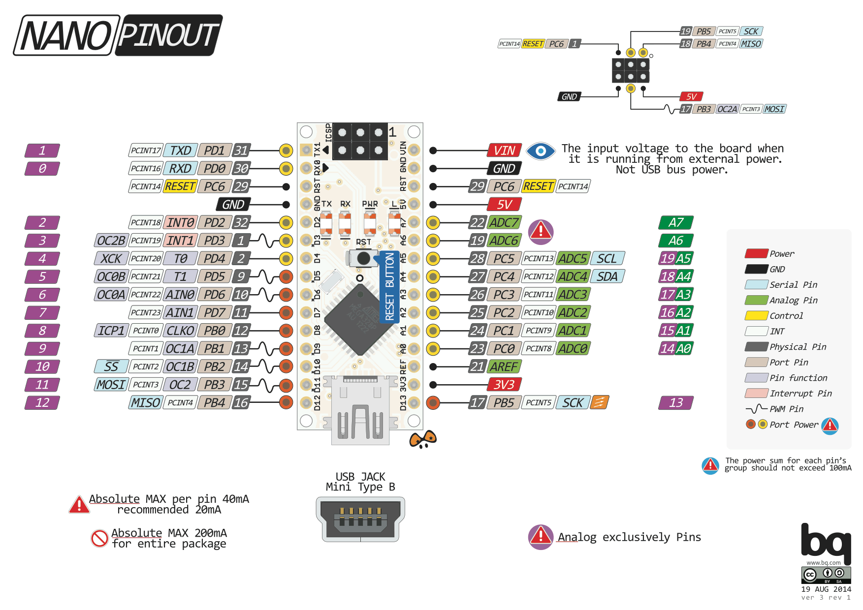
ATtiny84 GPIO Register Reference
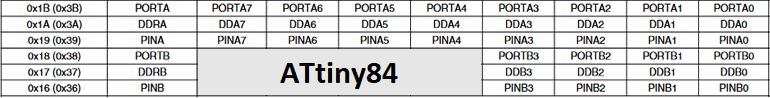
Register-Level Coding of the ATtiny84
Task.
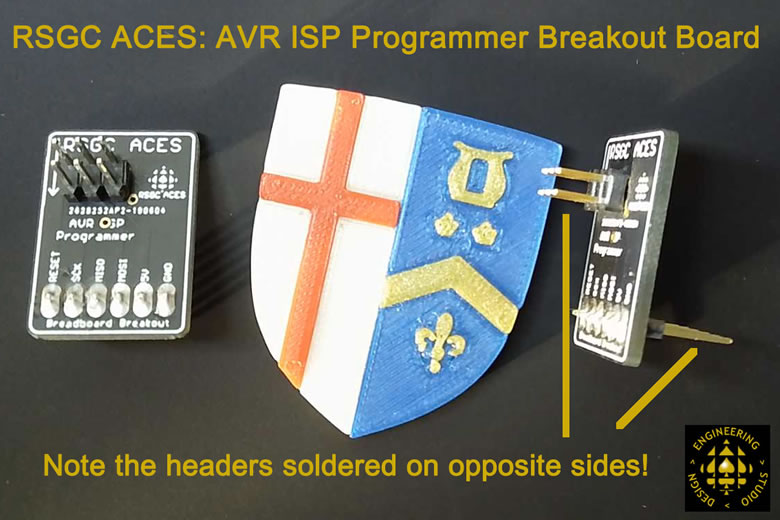 For the majority of next few months you'll be programming your ATtiny84 with your Sparkfun AVR Pocket Programmer (SAPP). Code is uploaded from the Arduino IDE through the Upload Using Programmer menu item within the Sketch menu (Ctrl+Shift+U). ISP connections with your ATtiny84 is accomplished with the support of the ACES AVR ISP Programmer BoB using the USBtinyISP (ATTinyCore) protocol selected with in the Tools>Programmer menu.
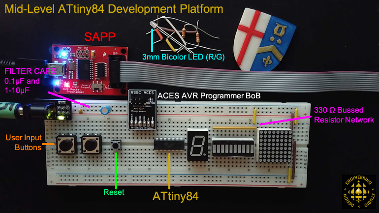
- Grab a free breadboard and assemble our Mid-Level ATtiny84 hardware platform modeled on the annotated photo below. The optical devices, from the 7-segment display to the right are not needed for this exercise. Your two 3mm bicolor LEDs in your loot bag, are. This layout, will, ultimately, provide a smooth transition to your Mid-Level Matrix Project due December 19th, or earlier.
- New MCUs directly from the factory are not quite compatible for breadboard use, in particular, their clock source. Select Tools>Burn Bootloader to set the correct clock source.
- In addition to configuring the clock source other features can be slected by setting parameters by fuses. Check out this useful AVR Fuse Calculator (link also found at the top of our course page)
- Be sure to wire the RESET pin with a 10 kΩ pull up resistor and a momentary button that creates a falling edge when pressed.
- Remember, this an MCU, so it's 5V, all the way!
- Create a new project called GPIOTests and drop in this code.
- This code is fully functional and we'll go though it, statement-by-statement. Your task is to comment each statement as to its purpose and/or function.
3. Mid-Level ATtiny84 Makeover of the Classic I/O Functions
 This is a large pool we're wading into, so let's start in the shallow end. Some of the first Arduino functions you were introduced to were pinMode(), digitalWrite(), digitalRead(), and shiftOut(). Those simple blinking LEDs provided early, but important, confirmation that your software and hardware efforts were meshing, and on the right track. The only problem was that there was too much 'behind the curtain' magic that, over a year later, we need to explore in order to optimize our future engineering objectives.
Task.
- Review the other graphic assets provided on this page above to wire up your AVR Programming BoB and your ATtiny84. Use the silkscreen printing on the AVR ISP Programmer BoB to direct your six essential connections.
- Wire in the RESET function of the ATtiny84 in the same manner as you did your standalone ATmega328P last year, with a 10 kΩ pullup resistor to the small 5mm ground momentary button, shown.
- In keeping with the "Honey, I shrunk my MCU", your Session 4 loot bag contains a couple of 3mm bicolor LEDs (even LEDs are smaller from here on in). Place one of them so that it spans the ATtiny84's digital pins 9 and 10.
- Create a project called MidLevelFunctionEquivalents and drop in this shell.
- This is your first official sketch destined for the ATtiny84 so, within the Board Manager dialog, ensure you have the latest version of Spence Konde's ATtinyCore installed.
- You'll be using your Sparkfun AVR Pocket Programmer (SAPP) with your BoB for these exercises so make sure you have USBtinyISP (ATtinyCore) selected as your programmer.
- Under the Sketch menu, select Upload Using Programmer to flash this code shell. Debug as necessary.
- Now, examine the code. You need to write the bodies of the three functions, using direct references to the GPIO #defines (iotnx4.h) in order to the have the bicolor LED alternately flash red and green. To make the logical connection between what the new functions need to do, I've simply swapped the names, as follows: modePin() replaces pinMode(), writeDigital() replaces digitalWrite(). and readDigital() replaces digitalRead().
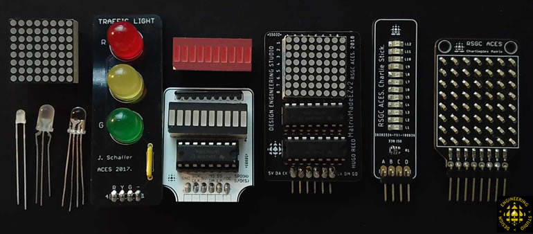
These are some of the familiar ACES optical devices we'll apply our nascent mid-level coding practices to ...
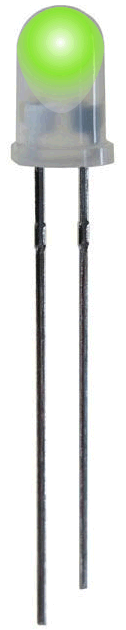
5. 3mm Red/Green Bicolor LED.
Your Session 4 loot bag includes two 3mm bicolor LEDs (red/green). Place its two leads in PA6-7, with the longer lead in PA6.
Create the project BicolorAlternation that employs direct, register-level GPIO Port manipulation resulting in red/green alternate flashing every half second.
 6. PlayByte. 5mm Red/Blue Bicolor LED.
 Your Session 4 loot bag also includes a 5mm bicolor LED (red/blue). Place its three leads in PA0-2, with the second longest lead in PA0.
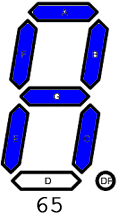
Create the project PlayByte that employs direct, register-level GPIO Port manipulation resulting in a continuous, 8-frame animated sequence that 'plays' a byte in an LSBFIRST order. The code is to be Red for 0 and Blue for 1. Each colour is to be held for 1 second, with no delay or gap in between. At the end of the 8-bit colour sequence, turn the LEDs off for 3 seconds before repeating, indefinitely.
Example. The image (above right) reflects the playing of B10011101 (or 0x9D or 0235 or 157).
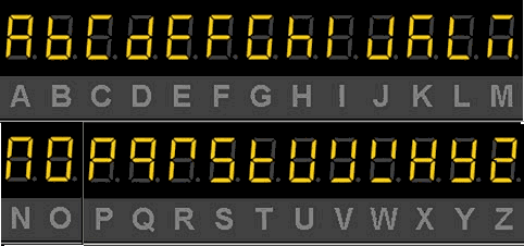
7. ASCII Alphabet on a 7-Segment Display.
 Your ICS3U experience introduced you to the concept of a segment map (array) for an ASCII letter lookup table (LuT). The code can be found at
  AVRFoundations: Write7SegUpperCaseCharacters.ino.
Obtain the array code for the segment map and drop it into a new project entitled ASCIIAlphabet. Develop register-level code that makes optimum use and efficiency of the ATtiny84's ports to continuously cycle through the LuT, displaying the letter representation on your 7-segment display device.
8. 10-LED Bargraph.
 (The ATtiny84 is just that, tiny, so this exercise may push the limits of the MCUs GPIOs). Create the project BargraphAnimation that uses a 1:1 GPIO port pin to LED mapping to duplicate the animation depicted in the image to the right. Strive to make it as efficient as possible.
9. Register-Level 74HC595 Shiftout (Morland Bargraph).
 The previous exercise left little GPIO room for anything else. We need to drive a 10-LED bargraph with fewer port pins, so we return to the 74HC595 shift register. However, in this iteration, we forego the use of the core shiftOut() function in favour of our own register-level bit manipulation strategy.
First, review the primer below on the 75HC595.
Create the project ShiftOutAnimation that duplicates the result of the previous exercise but only requires three ATtiny84 GPIO pins, as opposed to ten.
10. 64-LED 2D Matrix.
 11. ACES' CharlieStick. TBC.
 12. ACES CharlieMatrix. TBC.
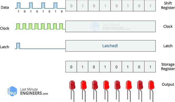
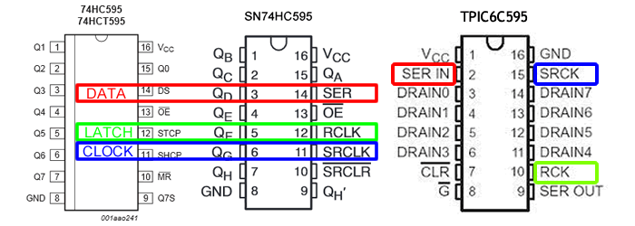
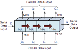 A shift register is a device typically used to expand the number of pins of a microcontroller. The most common design by far is based on the 74HC595 architecture. Using (as few as) three pins of the MCU (coloured) you are able to control 8 (or more) data lines (QA..QH). In addition to the three pins that control shifting, two other pins (Output Enable and Master Reset) provide additional (Active Low) control over the state of the 8-stage internal register set and output latches.
The IC accepts bits serially and presents them on output pins in parallel.
Two sets of naming conventions for pins tend to confuse those new to the IC. The image below tries to address this issue.
2. Waveform Timing Details. The digital orchestration of serial input bit stream is summarized in a waveform or timing diagram. A more detailed explanation of the mechanics of Serial to Parallel Shifting-Out with the 74HC595 can be found by following the link to the Arduino tutorial. Let's attempt to decipher the timing diagram, extracted from the 74HC595 datasheet,
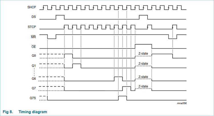
As you are well aware, the immediate benefit of the Arduino shiftOut function is to hide the details of the digital dance allowing the higher-level programmer to concentrate on more macro concepts. However, hiding details always comes at a cost; if not performance then, at the least, in understanding. Our goal is to solidify our lower-level coding skills through direct handling of the signals on the three control pins, thereby bringing you closer to the AVR and IC hardware. This brings all sorts of future dividends.
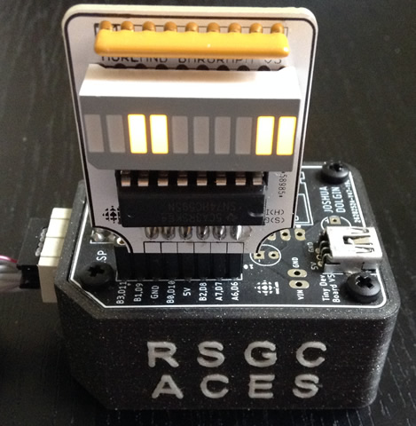 3. Prototyping Platform. Insert your Morland Bargraph into the DDP in the most feature-suitable position (supply and PWM) as shown to the right.
4. Register-Level shiftout. With the signals and waveforms of the 74HC595's timing diagram understood, we can now tackle the low-level responsibilities of the waveform ourselves through direct register manipulation. Remember, our goal is to enlighten, not suggest this is the preferred alternative in all cases.
- The function syntax we're going to simplify that conventional
shiftOut header function. We'll use a purely lowercase shiftout to avoid compiler confusion,
// LSBFIRST:0 MSBFIRST:1
void shiftout(uint8_t order, uint8_t value)
Complete the body of the function, hard-coding the port manipulation for this platform.
- Add code to your
loop() function that exercises your shiftout() function to display an interesting pattern on the bargraph.
- Questions worth considering: Where is the power coming from to drive the LEDs? Does it come directly from the MCU or does it come from the 595's output pins? What are the maximum voltage and current capabilities in either case?
Not surprisingly it's an important point that was answered pretty well on this forum...

