 There are no quizzes, tests, or exams in our ACES program. Put another way, you are NEVER put into the position of having a dramatically limited amount of time to demonstrate the skills you have acquired. Life is seldom like that. On the contrary, you are free to invest as much (or as little) time into your projects and reports as YOU choose. In return for being granted complete control over the depth and quality of your submissions I will place a premium on detail, precision, and the pursuit of perfection. So, my advice to you if you want to become exceptional is to follow the written and oral instructions carefully and, beyond the required elements of each report, demonstrate tasteful and appropriate creativity and imagination to distinguish yourself from the mediocre. Good luck and, remember, the race is long but it's over quickly.
Reports. Required Elements
If you do not submit your report by the deadline specified, you receive a mark of 0. This is done as a favour to you to help you appreciate that the real world will dismiss you if you can not demonstrate responsibility and accountability. You are to archive ALL of your reports in the single Word document, DER.docx. The first page is your Title page, followed by a multi-page Table of Contents, after which your reports begin. EACH report will start at the top of the next new page and, unless otherwise specified, consist of the following sections, in the order listed,
Theory
Purpose
Reference
Procedure
Media
Reflection
The vast majority of us can tell the difference between quality and rubbish in an instant. As a young scholar you have to decide what your name will stand for. It should matter very little whether you enjoy a task or not; if you're going to attach your name to something it is a direct reflection of who you are.
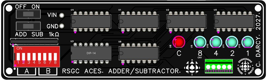
Project 1.3 Adder/Subtracter ( for Spring 2027)
Junior ACES are given the opportunity to solidify their new found skill set through the development of an extended prototype/device project. The Adder/Subtracter is the latest entry in the Culminating Project suite, after the Counting Circuit and the Minute Minder.
Our first course has introduced you to adder circuits of unsigned integers that exploit the logic functions to produce sums of binary operands. This project uses similar circuitry to perform both addition and subtraction of signed (2's Complement) integers.
A. Negation: 2's Complement
TBD...
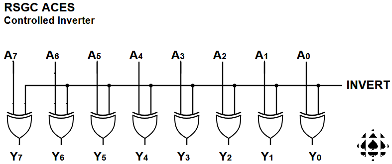
To achieve the 1's complement (or simply, the complement) of a bit, an XOR gate is employed. An additional bit can be used to control the inversion. If the INVERT bit is LOW, the A input bit passes unchanged. If the INVERT bit is HIGH, the A input is inverted. The schematic below depicts an 8-bit controlled inverter.
For example, if the input byte is A7..A0=0111 0101 and the INVERT bit is LOW, the output is Y7..Y0=0111 0101. However, if the INVERT bit is HIGH, the output is Y7..Y0=1000 1010.
Discuss these concepts in your Report.
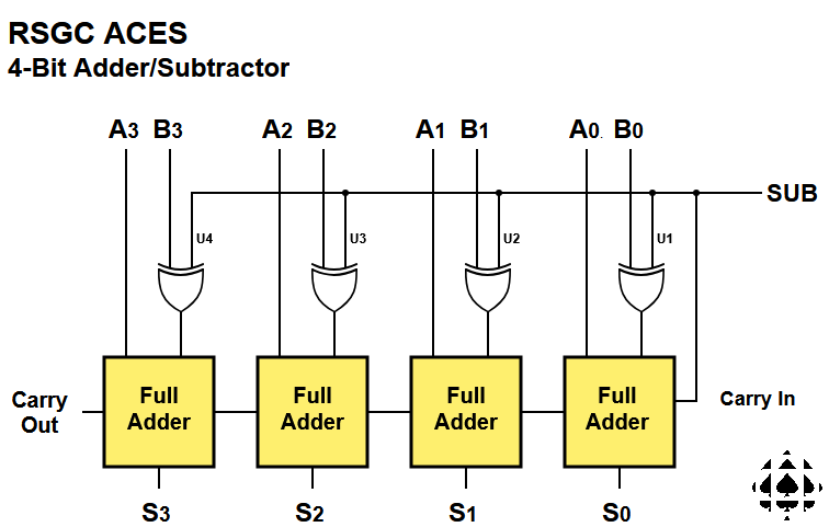
B. Adder/Subtracter Schematic
The schematic for the 4-bit Adder/Subtracter circuit appears below. It makes use of the controlled inverter subcircuit that your Report should discuss in relation to Part A above. SUB acts as the INVERT control bit for the 1's complement. A Full Adder replaces the Half Adder for the least significant bit position to to accept the addition of a 1 to achieve the full 2's complement form required to negate the subtrahend.

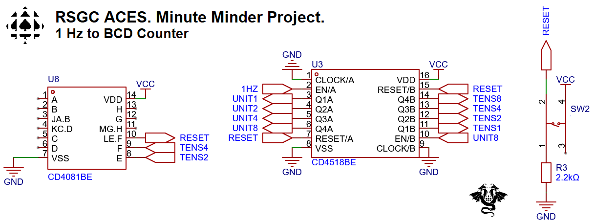
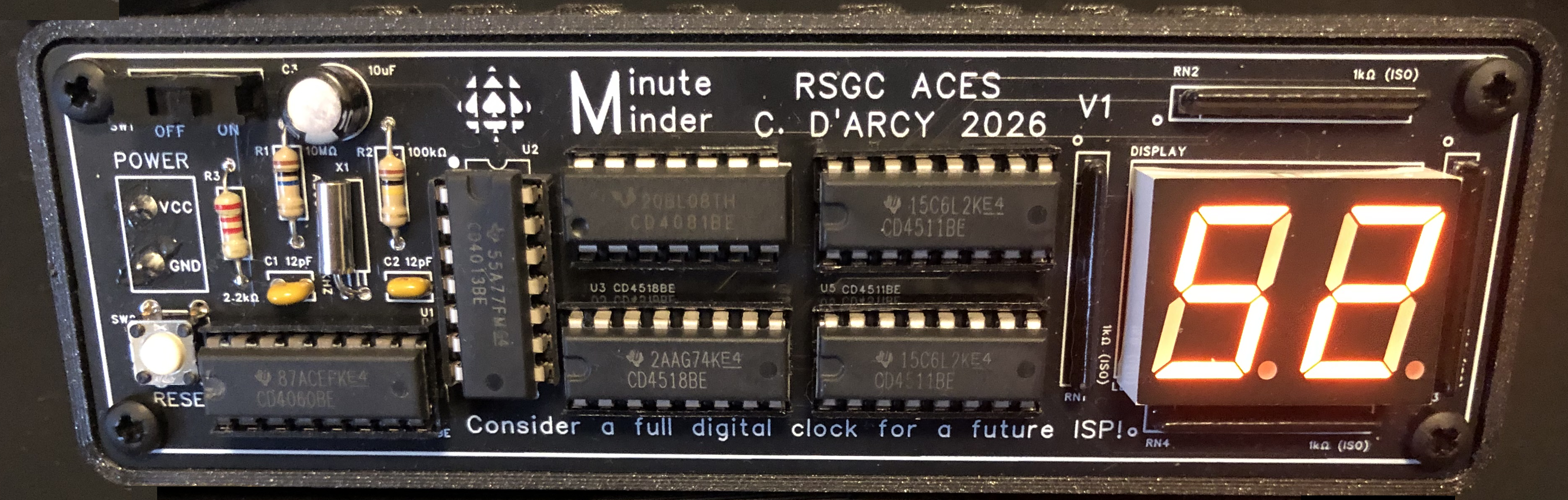
Project 1.3 Minute Minder
In lieu of a final exam Junior ACES are asked to undertake a massive, multi-stage project over an extended period of time designed to advance both their hard and soft engineering skill sets. Developing a complex prototype and DER in parallel steps promotes strong time-management skills and introduces you to the strategy of breaking large tasks into a sequence of smaller steps. You see, for the bulk of your educational experience courses break down responsibilities for large tasks for you, thereby shielding you from the opportunity of planning, commitment, organization and task management. Not this time. This experience provides a strong model for your ISP projects in Years 2 and 3 of our ACES program.
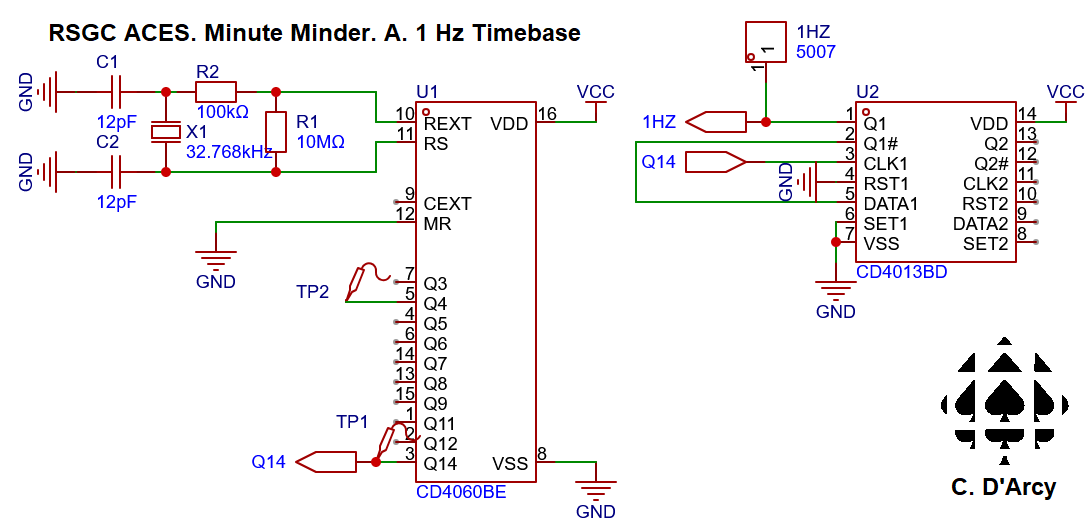
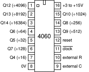
This device is designed to present an accurate count of the seconds within a minute. The digital count is presented continuously from 00 to 59. At its core is a 32.768 kHz quartz tuning fork crystal.
A. Accurate 1 Hz Timebase
-
Purpose
- Theory. Explain the relationship between a quartz crystal and electricity.
- Procedure. Explain the two ICs. Explain how the CD4060 and CD4013 cooperate to achieve a 1 Hz clock signal from the 32.768 kHz quartz crystal. Include a specific parts table, pin diagrams for required ICs and a schematic. Support with well-composed and well-formatted photos.
- Reflection
B. Binary Coded Decimal (BCD) Counting
-
Purpose
- Theory. Explain BCD Encoding
- Procedure. Include a specific parts table, pin diagrams for required ICs and a schematic. Support with well-composed and well-formatted photos that include 8 (temporary) LEDs to confirm the BCD counting.
- Reflection
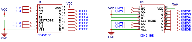
C. BCD to 7-Segment Decoding
-
Purpose
- Procedure. Include a specific parts table, pin diagrams for required ICs and a schematic. Support with well-composed and well-formatted photos.
- Reflection
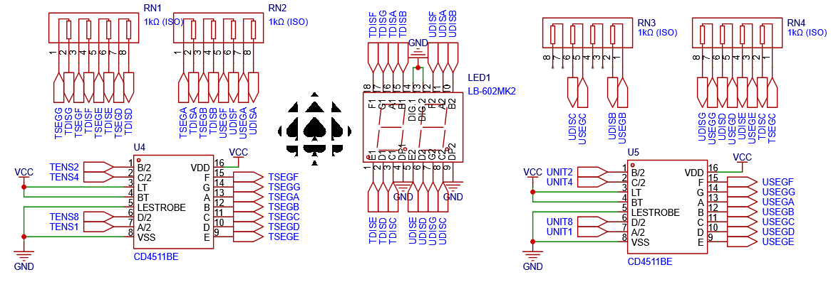
D. Dual 7-Segment Display
-
Purpose
- Procedure. Include a specific parts table, pin diagrams for required parts and a schematic. Support with well-composed and well-formatted photos.
- Reflection
E. PCB Assembly and Confirmation
Note: Due to both the time constraints and the cost of the components only those students with a working prototype by the start of class on Tuesday May 19th will be given the parts to continue to assemble the final device.
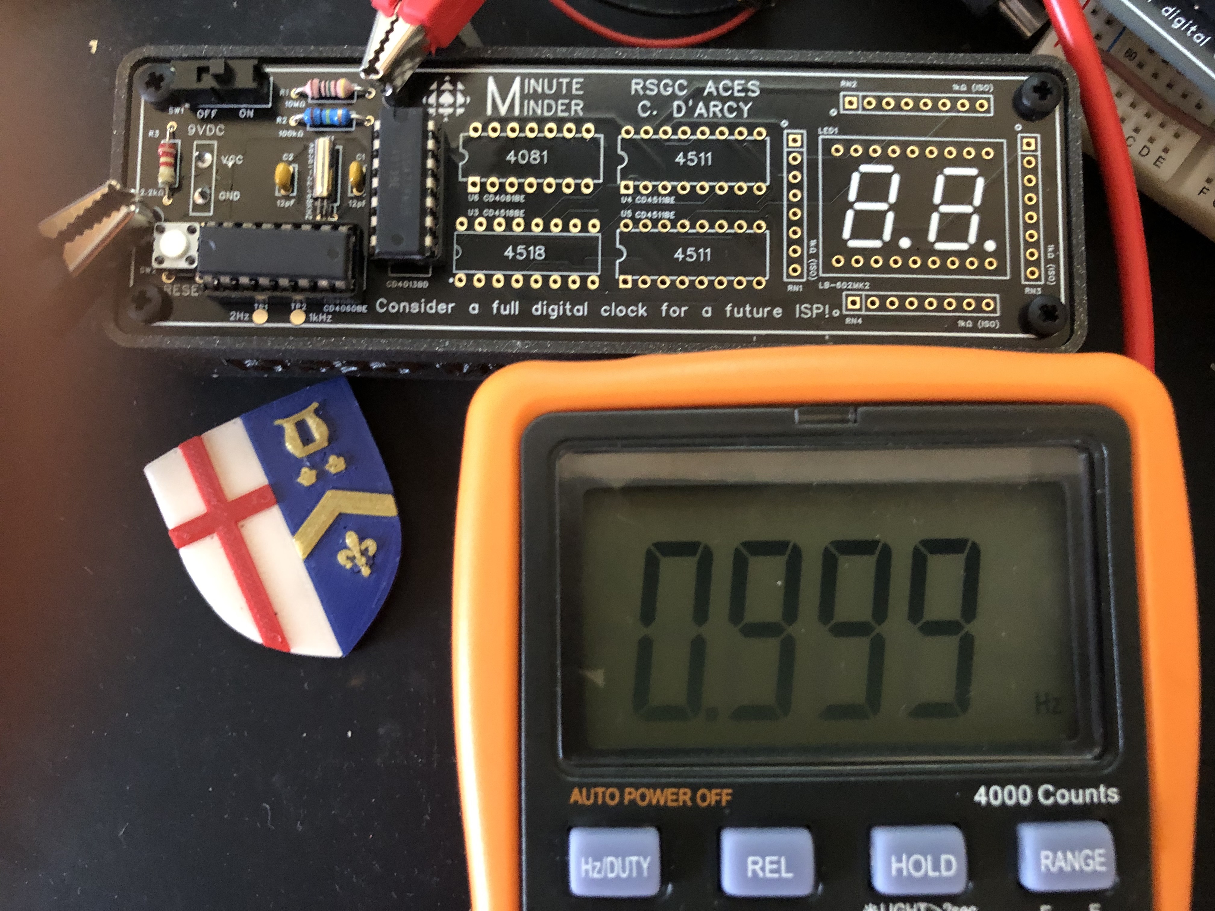
PCB Assembly will be undertaken in TWO stages, with confirmation of the first stage required to receive the parts for the second stage (again, for both practical and cost reasons). For the first soldering stage a DMM must confirm the three frequencies (2 Hz, 1 kHz and 1 Hz) at the respective Test Points (see photo below). Present this to Mr. D. to receive the balance of the parts.
-
Purpose
- Procedure
- Include a specific parts table and PCB image
- Include a discussion, measurements and confirming DMM photos at the three Test Points,
- TP1-GND (2 Hz)
- TP2-GND (1 kHz)
- TP3-GND (1 Hz)
- Support all with well-composed and well-formatted photos.
- Reflection
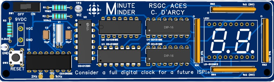
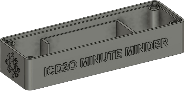
F. Encasement
-
Purpose
- Procedure. Include a specific parts table and case image. Support with well-composed and one or two well-formatted photos.
- Reflection
G. DER
 Your DER starts with a (big picture) Theory section,
written in your own words that mentions, generally, the input to the system, the generation of a frequency that is divided down, processed through stages, and culminates in the presentation of time count on the dual display device.
Your DER starts with a (big picture) Theory section,
written in your own words that mentions, generally, the input to the system, the generation of a frequency that is divided down, processed through stages, and culminates in the presentation of time count on the dual display device.
Click on the Navigation Pane on the right to see how your Report should be structured.
A Note on Graphics. Graphics should support the text they are illuminating. Poorly composed photos, sloppy and inconsistent choices for diagrams like pinouts and schematics work against you as they can confuse your readers and leave them with a sense that if the author doesn't care about his presentation why should they?
- Media. Include a final Media section with the link to your Youtube Video summary of each of the stages and a few never before seen photos.
- Reflection. Final thoughts on the project and the course.

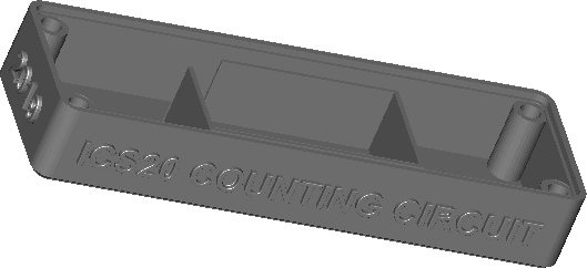
Project 1.3 A Counting Circuit
 Start your DER with a big picture Theory section,
written in your own words that mentions, generally, the input to the system, the generation of a clock signal consisting of pulses having both a duration and a frequency, culminating in the presentation of the pulse count on the display device. This would also be an ideal place to present a detailed, margin-to-margin, (Fritzing or TinkerCAD) breadboard or (organized) schematic view, to introduce your readers to the full prototype you are about to describe and discuss in multiple pages that follow.
Start your DER with a big picture Theory section,
written in your own words that mentions, generally, the input to the system, the generation of a clock signal consisting of pulses having both a duration and a frequency, culminating in the presentation of the pulse count on the display device. This would also be an ideal place to present a detailed, margin-to-margin, (Fritzing or TinkerCAD) breadboard or (organized) schematic view, to introduce your readers to the full prototype you are about to describe and discuss in multiple pages that follow.
A Note on Graphics. Graphics should support the text they are illuminating. Poorly composed photos, sloppy and inconsistent choices for diagrams like pinouts and schematics work against you as they can confuse your readers and leave them with a sense that the author doesn't care about his presentation so why should they?
Follow the Theory Section with the eight subsections (A-H) described below. For the first section, Analog Input, include, as a graphic, that part of the schematic that it pertains to. The next five sections (B-F) subsections should include a Reference Section that includes the respective live hyperlink appearing below:
Following the Reference Subsection within each of the five areas, include a Purpose section (this one could go before the Reference Section)
describing in detail, how each stage contributes to the sequence. Be sure to clearly present the input, processing, and output of each stage, supported by informative, attractive, and well-formatted graphics.
Following the final subsections include Media (captioned photos and video) and Reflection sections.
A. Button Input
- Purpose (discuss the momentary PBNO and its pullup resistor configuration)
- Include your own breadboard/schematic diagram, right-aligned, to
support your discussion.
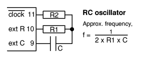
B. NAND Gate Oscillator (4011)
- Purpose
- One or two sentences explaining the role this stage has within the complete circuit.
- Procedure
- Explain, in detail, the function of this chip (Input, Processor, Output)
- Explain the concept of analog input to digital output and how this
chip accomplished this
- Include
a discussion of the pin diagram in this
IC
- Explain what a clock signal is
- Discuss the role played by RC1 and RC2 and the role played by its respective capacitors and resistors.
- Pinout diagram taken from the web and your own breadboard /schematic of the wiring and supportive passive (analog) components
C. Decade Counter (4017)
- Purpose
- One or two sentences explaining the role this stage has within the complete circuit.
- Procedure
- Explain, in detail, the function of this chip (Input, Processor, Output)
- Explain what it means to ensure ALL of the input pins must be conditioned and
how this is done
- Pinout diagram taken from the web and your own breadboard /schematic of the wiring.
D. Decimal Counting Binary Up/Down Counter (4510)
- Purpose
- One or two sentences explaining the role this stage has within the complete circuit.
- Procedure
- Explain, in detail, the function of this chip (Input, Processor, Output)
- Create a two-column table with rows for all 16 4-bit binary values in the
left column and their equivalent decimal values in the right column
- Pinout diagram taken from the web
E. Binary Counting Decimal Decoder (4511)
- Purpose
- One or two sentences explaining the role this stage has within the complete circuit.
- Procedure
- Explain, in detail, the function of this chip (Input, Processor, Output)
- Explain the purpose of the Blank, Store, and LampTest pins and how they must
be conditioned for normal use.
- Pinout diagram taken from the web
F. Seven-Segment Display
- Purpose
- One or two sentences explaining the role this stage has within the complete circuit.
- Procedure
- Explain, in detail, the function of this component
- Explain the difference between the Common Anode (CA) and Common Cathode (CC)
versions of this component. Which one did we use?
- Explain how the pins on the 4511 and 7-seven segment make the wiring straightforward.
- Explain why each pin on the display requires its own resistor.
- Graphic (google a similar small image)
- Pinout diagram taken from the web
G. A Counting Circuit PCB
Once the breadboard prototype media has been obtained for your DER (photos and video), ACES are to convert their prototype to a more permanent device. A custom printed circuit board was designed and manufactured expressly for the use by Jr. ACES for this purpose. Supplemental parts provided by Mr. D. appear in the table to the right.
Interested ACES should present their working prototype to Mr. D'Arcy at least TWO days prior to the DER due date in order to receive their PCB and supplemental parts. Receipt of such a board comes with the expectation that components will be soldered, the circuit tested, and summarized in text, photos, and video as part of the DER summary for this Counting Circuit project.
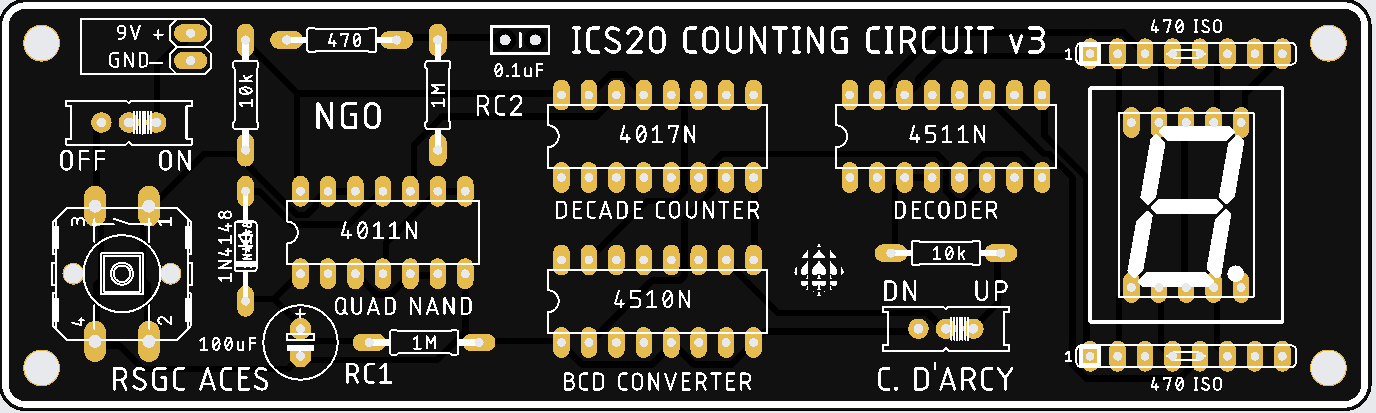
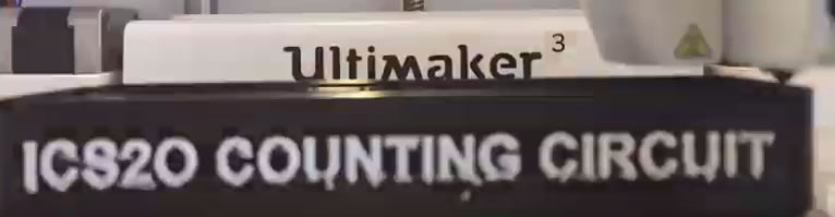
H. A Counting Circuit PCB Case
 Congratulations on reaching the final stage (8) of our marathon Counting Circuit project! Students that have successfully soldered their PCBs that demonstrate forward (and backwards) counting on the seven-segment display are invited to present their circuit to Mr. D. to receive a custom case designed and printed in the DES by J. Dolgin (ACES '20) into which their device can be mounted. A similar two-colour case was printed on the Ultimaker 3 in 2018 by K. Fiset-Algarvio (ACES '19). Click the image below to view a short time-lapse video of the case being printed,
Power for the device is sourced from a 9V battery inside a compartment within the interior of the case. The leads of a battery snap can be soldered to the correct pads in lieu of an external DC Jack. Be sure to place electrical tape across the battery to insulate it from the bottom of your PCB to prevent the possibility of shorting. Finally, screw the assembly together and fully test, prior to capturing the final frames of your project video.
Finally, be sure to address ALL issues from previous submissions and update your Table of Contents before attaching DER.docx to an email to ACESHandin@rsgc.on.ca under the Subject Line: A Counting Circuit
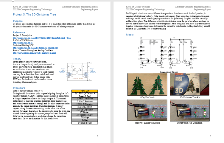
 Project 1.3 ACES Christmas Tree
 In addition to recently-introduced digital logic gates, the CMOS family offers a wide range of specialized ICs. One such terrific chip in the oscillator/counter category is the 4060, that uses a 'programmable' oscillator as a clock source, by dividing its frequency by specific factors and presents these signals on its output pins. The 'programming' of the 4060 is achieved through the use of three external analog components (two resistors and a capacitor). Finally, the suggestion on the Electronics' Club's site that this could be put to good use in creating a Christmas decoration was too compelling for us to resist! So, here we are...
Good References:
The Procedure section of your Report on this project will be organized into FOUR subsections, one for each task described below.
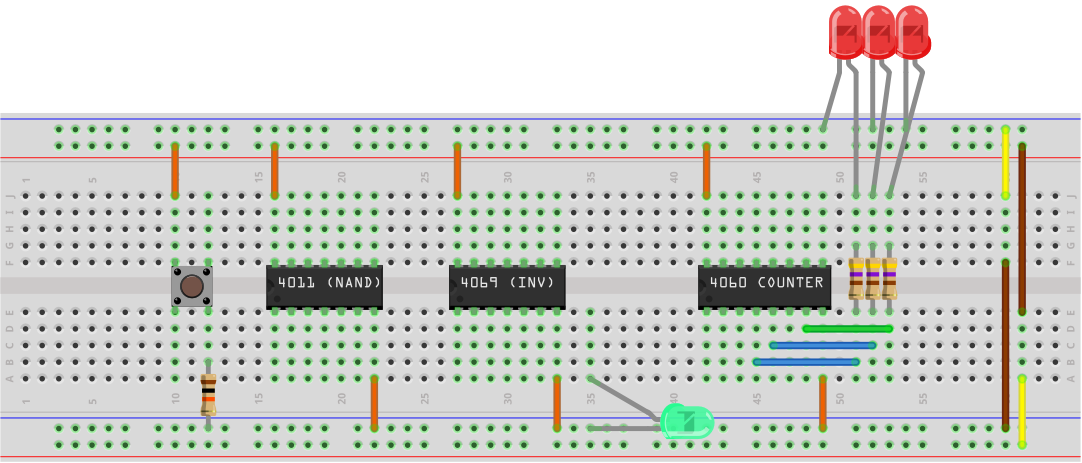
1. RC Oscillator
- It is instructive to create an RC oscillator similar to the internal 4060 for yourself. Click on the image below and examine the Falstad simulation carefully.
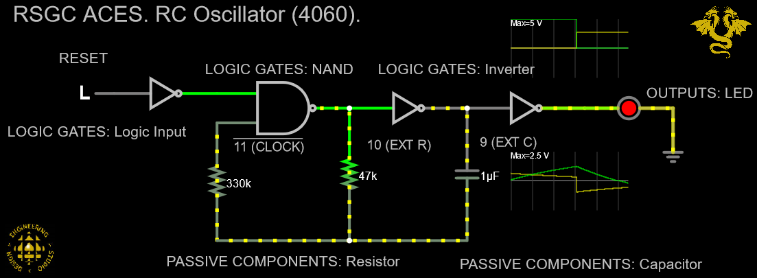
- Using the EXACT layout as shown below, implement the RC Oscillator shown above. The LED should be flashing.
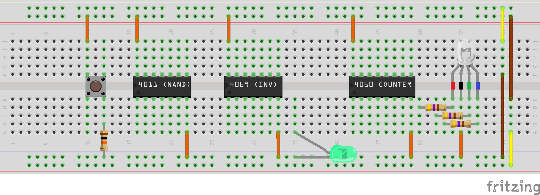
- Be sure to take some well-composed photos for your Report.
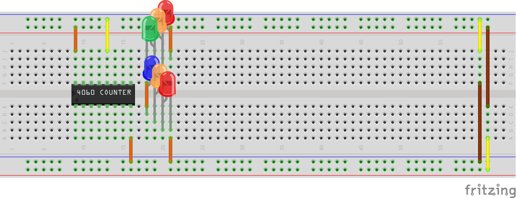
2. 4060 Counter/Frequency Divider
Here is a Falstad simulation of how a Frequency Divider IC (like the 4060) can create the illusion of Binary Counting:
https://tinyurl.com/2yj5tytf
 Using the same external analog components from Step 1 (C:1 μF, R1:47 kΩ, R2:330 kΩ) develop a breadboard prototype that exploits the 4060 to present three clock signals (square waves) of varying frequencies on three LEDs to provide an illusion of counting in colours. Feel free to experiment with different programming combinations of the fixed resistors and capacitors to achieve a compelling effect. Consider engaging a potentiometer allow for easy frequency adjustments.
- Using the values for C and R1 from above, include a mathematical presentation of the expected frequencies of the clock and the three 'divided' square waves, as discussed in class using this Excel Analysis
- While developing, be sure to obtain well-composed photos and video footage for your Report and accompanying video.
3. Multiple LED Strings
A single square wave, strategically positioned, can drive short strings of multiple LEDs in series.
- After deep consideration of this Falstad simulation of a frequency divider/counter IC like the 4060 driving multiple strings of LEDs, develop your own breadboard prototype of the circuit. Ideally you'll present four sets of 6-8 LEDs in series, driven by four outputs of the 4060 (Q4-Q7 work best).
4. The RSGC ACES Christmas Tree
It's time to assemble the final device that places the conceptual foundation of the previous stages onto a custom PCB. The schematic below presents a rough idea of the design on the PCB that should look familiar (our Grade 11 ACES course introduces you to making your own custom PCBs).
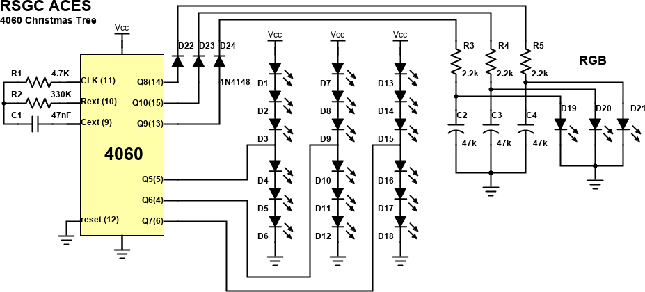
In Stage 4.1, I will provide
At this stage, first solder in the chip seat (without the 4060!) in the correct orientation. Next, solder in the Power Jack. Now insert your 4060 in the correct orientation. Apply 9V to the power jack and confirm your tree's functionality. Also, apply 9V to the positive and negative power pads that are below the 4060. Demonstrate your device to Mr. D'Arcy to receive the second round of supplemental parts.
The Stage 4.2 the new part(s) include,
 Seat the tree on a 9V battery to confirm functionality. Demonstrate to Mr. D.
In Stage 4.3 successful builders to this point will receive a special ACES 3D printed star diffuser and stand, both designed by S. Appleyard (ACES '23, Imperial College '27)
Create the most comprehensive Report you can and submit by the deadline. Don't forget to update your Table of Contents.
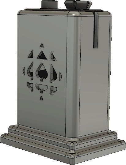
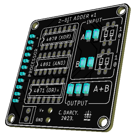
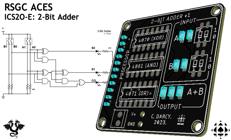
 Project 1.2 The 2-Bit Adder
Recently-completed class sessions have introduced you to digital logic gates. These are the computer's primary operators in much the same way as addition and multiplication are humans' primary arithmetic operators. One of many useful circuits involving logic gates are circuits that allow computers to perform addition of binary (base 2) numbers.
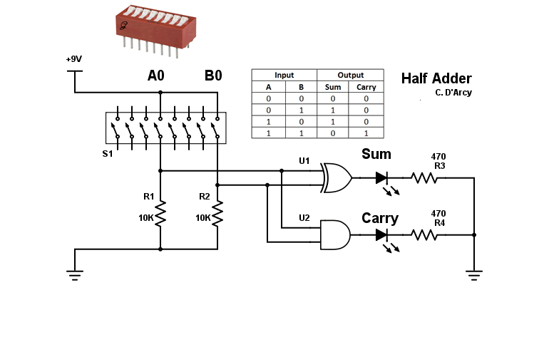
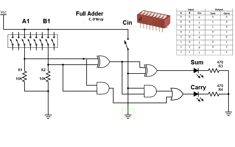
Background: Half- and Full-Adder Circuits
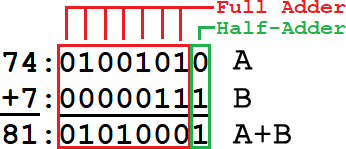 The graphic to the right is meant to reveal how the computer 'sees' the addition of 74 and 7, organized as 8-bit binary numbers. Similar to humans, the computer proceeds from right-to-left, adding pairs of binary numbers (0 and 1). For the first addition (green) there is no 'carry in' number from a previous addition. This requires a circuit known as the Half-Adder. For each of the remaining seven additions (red), the computer must add the two binary operands (A and B) but must also add in the binary number carried from the previous addition (C). A circuit that performs this is referred to as a Full-Adder.
Jr. ACES are not expected to have come up with the circuit designs for the Half- and Full-Adder circuits (although many of you likely could), but a strong grasp of why they work, and the correct outcomes they produce, provide deep mental satisfaction. To this end, you are encouraged to spend time interacting with the relevant combinational circuit examples provided as Falstad simulations in the table below.
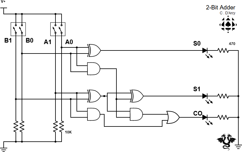
Task. The 2-Bit Adder Circuit
 With the Half- and Full-Adder circuits above as a foundation, a breadboard prototype capable of the addition of a pair of 2-bit operands can be achieved.
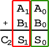
 - The graphic to the right is the goal of this circuit. A Half-Adder circuit is required to produce the sum of A0 and B0 (green), together with a carry bit to merge into a Full-Adder circuit to achieve the sum of A1 and B1 (red) with a carry bit, C2.
- The schematic for this circuit appears below.
- An RSGC ACES' Falstad simulation can be explored by following this link: https://tinyurl.com/2ymqmqzj.
- Breadboard prototype parts will include 4 push buttons (or slide switches) for inputs A and B input pairs, three LEDs for outputs, and the required CMOS ICs as the processor that integrates both a Half- and Full-Adder as the circuit below suggests.
- On Monday November 25 students presenting a working 2-Bit Adder breadboard prototype at the START OF CLASS will be supplied with the components required to assemble a 2-Bit Adder PCB.
- On Wednesday November 27, students presenting a functioning 2-Bit Adder PCB at the START OF CLASS will be supplied with a 3D printed case, and power jack. NOTE: Instructions will be provided in class on how to prepare your power jack and case.
DER Considerations
 Each new DER Project Summary starts at the top of a new page.
- Using the DER returned to you that has since been edited and corrected, and taking into account the personal and general feedback comments you have been provided with, start this report on first new page, after your previous report. Add the new Project name in Heading 1-Style and complete Heading 2-Style sections: Theory, Purpose, Reference, Procedure, Media, and Reflection. Within the Procedure Section add Heading 3-Style subheadings as shown on the Navigation Pane to the right. Support these subsections with the associated schematic and other graphic resources.
- Text is developed in accordance with the recommendations for Technical Writing and reflective of your much-improved formatting abilities. Graphic manipulation is undertaken according to the specifications laid out in the Design Engineering Report General Guidelines.
- Within the Procedure's subsection adapt a Supplementary Parts Table as I've provided in this Word document that is consistent with your previous preferred column organization and background shading theme.
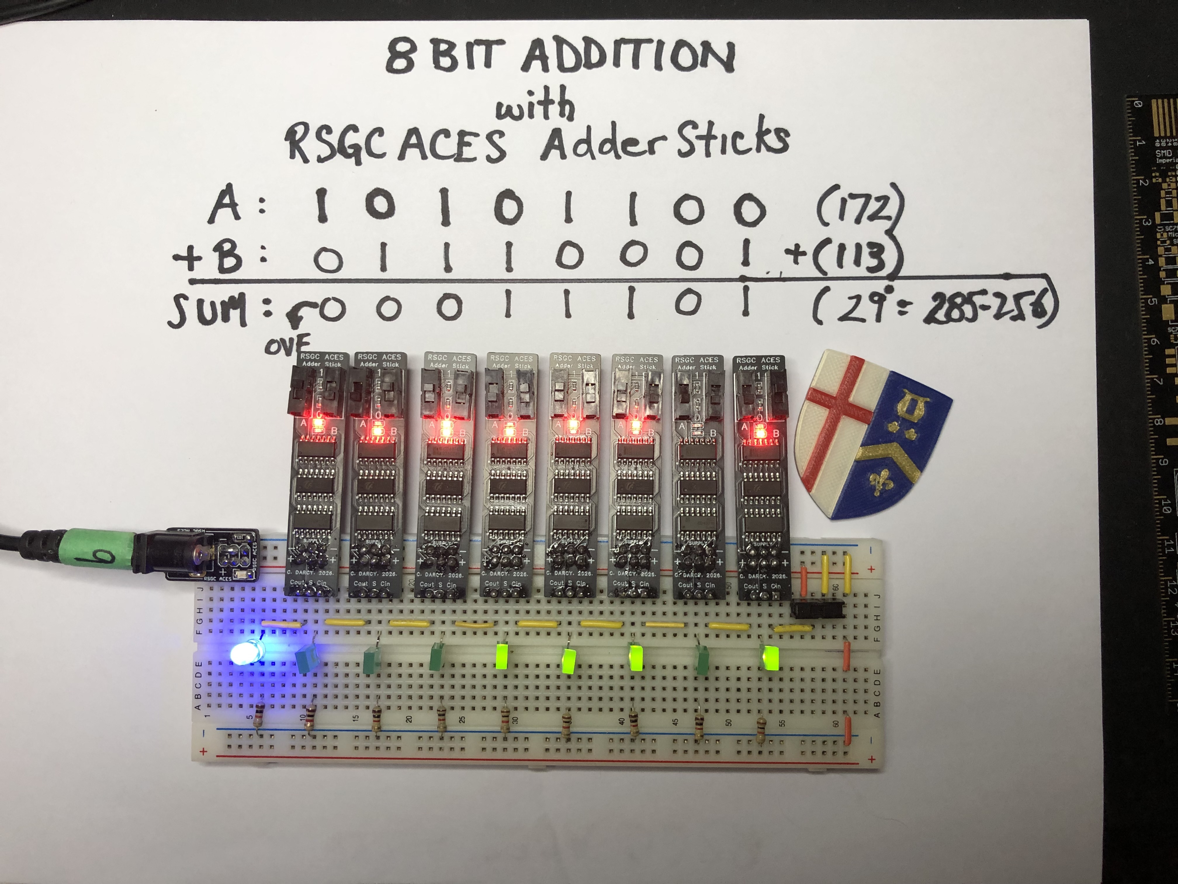
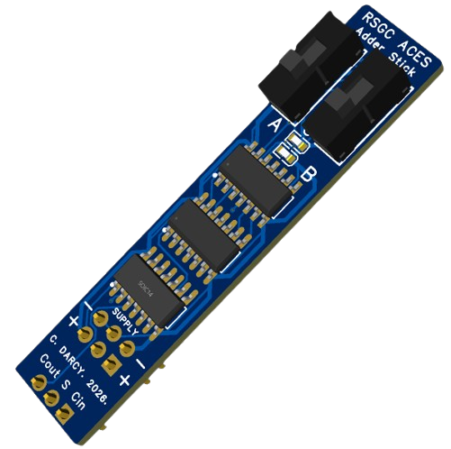
 Starting in the Fall of 2025 you are asked to combine the RSGC Adder Stick lent to you with FOUR of your peers and assemble a 5-bit Adder example, similar to the 8-bit Adder example shown here (http://darcy.rsgc.on.ca/ACES/TEL3M/images/8BitAdder.JPG). Each of the 5 group members may use the same common 5-bit image of their final result in their DER but their discussion of the process will be unique to them.
- Superior photos and video footage of your breadboard prototype (and encased PCB) are essential.
- Students should note that the mark you receive for this submission will be based on the clarity of your circuit presentations and quality of your DER based on your response to the expectations, feedback, and support previously provided you.
 Attach your DER to an email to handin with the Subject: The 2-Bit Adder by the deadline, at midnight.
8-Bit Addition with RSGC ACES' Adder Sticks
Project 1.? 1-Bit Magnitude Comparator
The vitality of our DES courses can be attributed to the achievements of the ACES that have preceded you. It is through their curiosity and commitment to their futures that we all benefit. It was J. Goodwin's (ACES' 22) 8-bit computer Medium ISP that inspired me to present this combinational logic circuit project to prepare you for what lies ahead.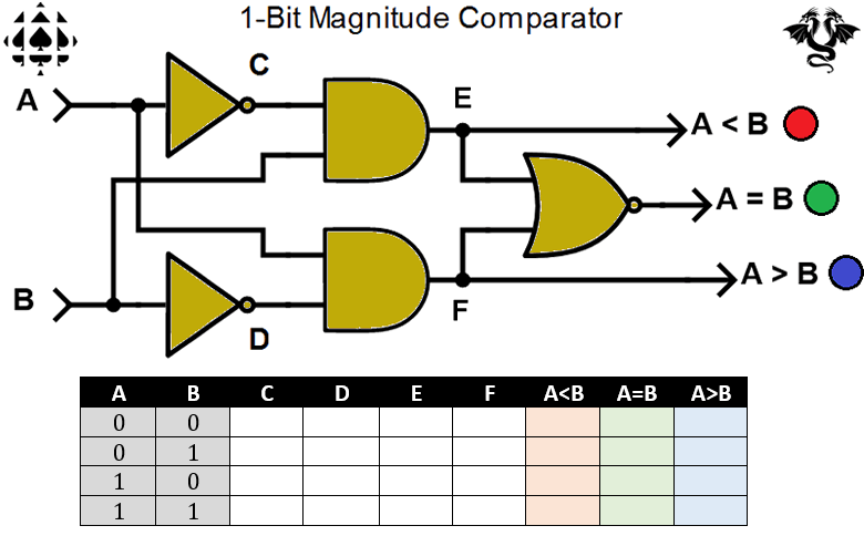
Modern digital technology is built on the foundation of Logic. On the back of a small set of logical operators (AND, OR, NOT, etc.) extraordinarily complex systems are constructed that enable all the devices we depend on. To begin your familiarity with these fundamental blocks you are asked to provide a circuit demonstration of a concept familiar to you: the relative magnitude (order) of (the two binary) digits: 0 and 1.
References
Task (Have your phone's camera available throughout the entire week to capture meaningful media for your Report)
- Develop a breadboard prototype of the combinational circuit above right. Here's a general layout you are encouraged to follow (simply because I have to figure out 26 prototypes)

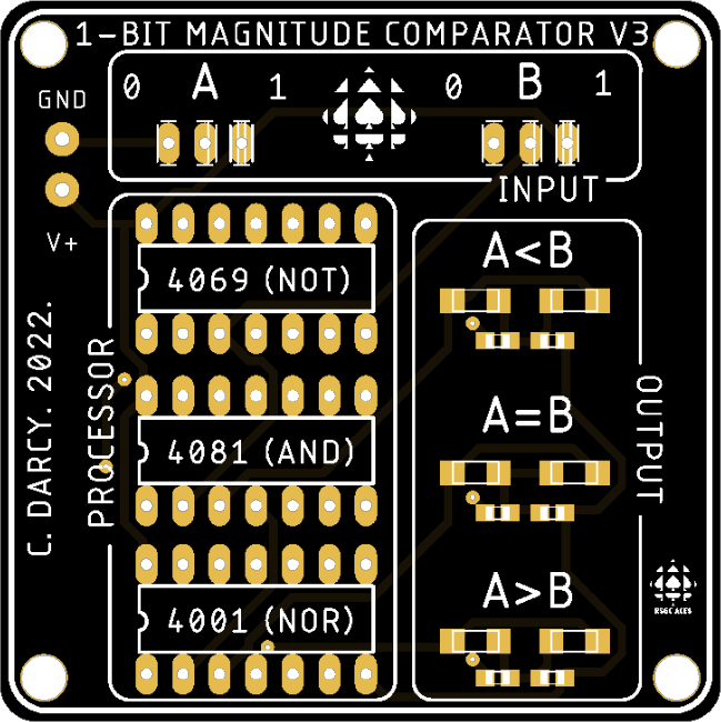 Two correctly conditioned slide switches are to be used for the inputs A and B.
- Since the three outcomes are mutually exclusive, your are to employ your COMMON CATHODE RGB LED as the sole indicator. Show RED for A<B, GREEN for A=B, and BLUE for A>B. Note: I recommend using no less than a 1 kΩ resistor (even going as high as 10 kΩ) as these can be blindingly bright.
- On the custom PCB you will be provided with for a successful prototype, I have used only red and green surface mount LEDs as indicators in pace of the RGB LED.
- For your Report, in addition to all the standard sections (Purpose, Reference, Theory, Procedure, Media, Reflection), you will include the following,
- Within an opening Theory section, explain the difference between combinational and sequential logic circuits.
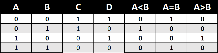
- Within your Procedure section, include the table below (you should make your own Word table with your preferred table shading theme rather than simply copying my graphic). C and D in the table below are intermediate results that can be resolved to better understand, determine, and summarize the circuit output in tabular form. Explain this in your Procedure Section.
- I recreated the circuit schematic from the reference provided above. You should do the same, using a schematic editor of your choice.
 Examine the circuit closely. It would not be obvious to many at first glance why is works but, if you push yourself to think about it, it becomes obvious and you should explain it (clearly), in your Procedure Section.
- In your Report, observe and comment on the behaviour of your circuit if the slide switches are simply removed from a functional circuit.
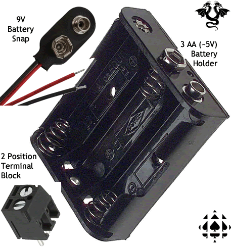
- Your final device will be powered with (approximately) 5 V. For the final assembly stage of the project you will be provided with 3 AA batteries and the supporting components that appear to the right. Once this is complete, four M3 screws and hex standoffs will be provided to serve as legs to elevate the comparator off the surface of your table. Note. For those that are continuing on to our Grade 11 course, you are encouraged to imagine and the many options there are for mounting PCBs if both a functional and aesthetic case or stand. This is why I provide you with these simple additional fasteners; to get you thinking about the elegant finish and polish of your projects.
 MS Excel offers the basic logic function (AND, OR, and NOT). See if you an duplicate the table below using these Excel logic functions that summarizes the 1-Bit Magnitude Comparator combinational circuit in this project. Remember, CTRL+` can be used to toggle the Excel views from Normal to Function and back again. A discussion of this would provide an enriched enhancement to your Report.
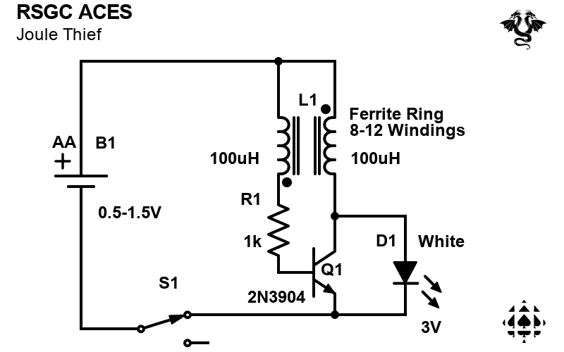
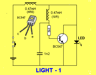
Project 1.2 Joule Thief (aka Blocking Oscillator)
 Joule is an SI unit of energy, named after James Prescott Joule in recognition of his discoveries relating heat and mechanics (thermodynamics).
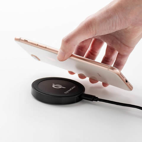
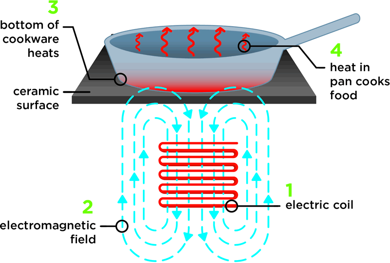
Wireless (inductive) phone chargers are commonplace. Advertisements for new cars often squeeze in an image of a deck onto which you place your phone for charging while cable-free. As the world reduces its reliance on fossil fuels, you'll likely see gas kitchen ranges replaced with those that operate on induction. Finally, those solar garden lights in your backyard are but another example of this principle. This project exposes you to the concept of electromagnetic induction in a fundamental circuit. You'll explore the theory further in your Physics course next year.
It's maddening (not to mention environmentally unfriendly) that 1.5V AA or AAA batteries are as good as useless in your TV remote even when when they still read 1.1V or more. It's time to get even with those stubborn cells by mining every last drop of potential they've got left in them before they head to Home Depot or Home Hardware for a proper recycling. Other names for this circuit can be found under Blocking Oscillator, Vampire Torch, Vampire Flashlight, and DC Boost Converter. Researching any of these phrases gives you a better understanding of the concept for your DER and may give some of you some great ideas for future ISPs. Here's a good video to start with,
 Why this Circuit Works when it Shouldn't.
 Stage 1. Look around your home for your stash of, so-called, 'spent' (0.5V-1.1V) AA batteries. Recall that fresh out of their package, they delivered about 1.6V. Mark them as USED and put one or two in your toolkit as you'll use them in this project.
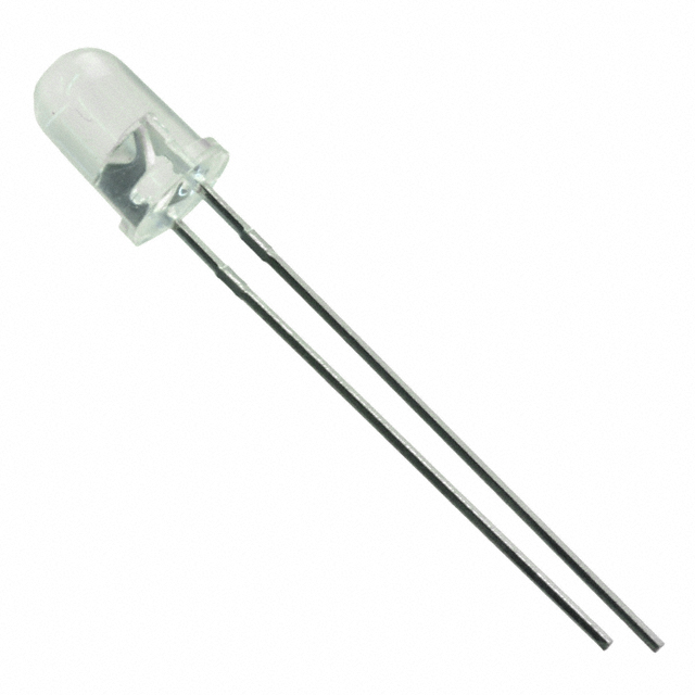
By now you are aware that voltage requirements for LEDs correspond closely with their relative position on the visible spectrum with RED requiring roughly 1.7 V to BLUE and BRIGHT WHITE pushing 2.4 V - 3.1 V.
Stage 2. Although it's a bit of a lost cause, see if you can light up any LED in your kit with one of those 'spent' AA batteries directly.
A review of the datasheet for the clear white LTW-2S3D8 LED pictured you have been provided with indicates, on page 4, that an average forward voltage of 2.8 V is required for this LED lamp to function normally. The purpose of the project is to take a minimal voltage source like your 'spent' AA battery and boost its voltage high enough to light the 2.8 V lamp. This is essentially the principle behind the ubiquitous solar garden light that has a 1.2 V rechargeable AA battery lighting its onboard LED at night. (see links below)
Research (it is recommended that you consider each of these steps prior to completing the required task)
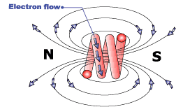
- Review a few principles relating electricity and magnetism: ACES' Frame Player: Field Forms
- Capacitors store charge in an ELECTRIC field whereas inductors store charge in a MAGNETIC field.
- An inductor can also be called a choke. Why might this term be appropriate?
- A boost converter is a device designed to increase voltage. What similar name is given to a device used to decrease voltage?
Stage 3. Few ACES tasks are as hands-on as this one, so prepare yourself...
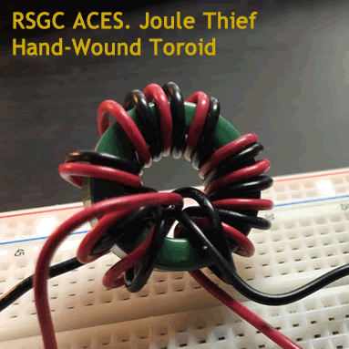
Inductor coils are employed throughout the electronics industry to increase and decrease voltage levels and are aptly referred to, generically, as transformers. Unlike the convenient pair of 100 μH axial inductors with built-in windings used in the upcoming PCB stage of our Joule Thief project, this stage requires you to hand-wind your own inductor coil around a toroid-shaped ferrite ring to generate the same effect on your breadboard prototype.
- Go to the 22 AWG wire rack at the back of the DES and cut off 16 in (40 cm) of two DIFFERENT wire colours of your choice. Use the ruler stick underneath the rack to measure them, prior to cutting.
- Your objective is to create a small transformer by winding the pair of wires around the toroid ring you have been lent. NOTE. The wire is sheathed and the toroid ring is enameled to prevent the bare metals from shorting the electromagnetic field and ensuing signals.
- Watch this video (or any one of hundreds) of the winding technique. Ten to twelve tight, NON-OVERLAPPING windings should do it. For the really keen ACE, check out this Toroid ring inductance calculator site. Yikes!
- After winding, use your wire strippers, employing the 22 AWG jaw, to strip off 0.5 cm of plastic sheathing from each of the four exposed ends to enable insertion into your breadboard.
Stage 4. Joule Thief: Breadboard Prototype
- Here is a good explanation for the operating principle of the Joule Thief taken from an Electrical Engineering forum, "Let's start with everything off and power newly applied. the transistor is off, so no collector current. However, there is a current path thru the resistor, the transformer secondary (the left coil), and the base of the transistor. This turns on the transistor, at least somewhat. The transistor turning on brings the bottom side of the primary (the right coil of the transformer) to a lower voltage than the power. At this point, the primary acts mostly like a inductor, so current builds up linearly over time. This change in current flowing out of the dot end of the primary causes the secondary to try to make current flowing into its dot end. This additional current through the secondary also means more base current, since the two are in series. More base current means the transistor turns on harder, which causes more current thru the primary, which causes more base current, which turns the transistor on harder, etc. Due to this positive feedback, the transistor is turned on so hard that its collector voltage can't go any lower, usually about 200 mV. That's called saturation. At this point, the transistor C-E junction looks like a closed switch, except for the small saturation voltage. With the fixed voltage of the supply minus the saturation voltage applied to the primary, its current ideally builds up linearly. However, it can't do that indefinitely. One of two things happen: The current levels off due to the inherent equivalent series resistance of the primary winding, or the transformer core magnetically saturates. Either way, the secondary is no longer driven to create higher current. Since a transformer works on the change of the magnetic field, the secondary stops providing additional base drive at all. Now the positive feedback works to quickly turn off the transistor. At first when the magnetic field levels off, the secondary no longer provides additional base drive, and the base current is just what the resistor allows to pass. That is not enough to sustain the same collector current, so the transistor starts to turn off a bit. This now reduces the magnetic field. The secondary now actively opposes the base drive provided by the resistor. The transistor allows less current, which causes more active negative base drive, which causes even less collector current, etc. Due to this positive feedback, the transistor turns off hard quickly. The primary now acts like a inductor. Its current can't be turned off instantly. The inductor makes whatever voltage it has to to maintain the same current instantaneously. The voltage rises quickly, and when it gets to the LED forward voltage, the current flows thru the LED and the voltage stays roughly fixed. The inductor now has reverse voltage across it, so the current thru it is decreased. Eventually it gets to 0, the magnetic field stops changing, the secondary stops opposing the current through the resistor, and we're back to about the state where power was first applied."
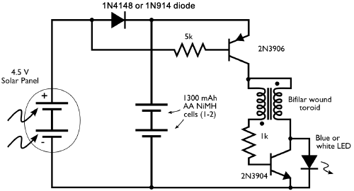
- Breadboard the schematic of the Joule Thief provided below, left.
- Notice the DOTS on the winding coils. This is meant to reinforce the requirement that OPPOSITE ends of the wire pair are placed into the positive supply rail.
- Be sure to capture compelling media for your DER and video in the process. The toroid ring is a large component so make sure your take your media from a strategic angle.
 |
 |
Stage 5. The Final Device
After capturing a number of photos and video footage for your DER you are ready to move from your temporary breadboard prototype to a permanent Joule Thief device.
-
Look over the additional parts you have been supplied with for this stage.
- You are to supply the resistor, transistor, slide switch, and battery. For this device, your AA battery voltage should be betwen 0.7 and 0.9 DCV.
- Carefully solder the inductors, resistor, transistor, slide switch and LED, in that order. Take care as there are no replacement parts for careless attention to detail.
- Take the Keystone #2561 AA Battery Holder (leads) you were supplied with for your breadboard prototype and confirm your Joule Thief is functioning.
- Present it to Mr. D. for confirmation to receive your PC Pin AA Battery Holder as the FINAL soldering task of your permanent device.
Stage 6. (For the Highly Inspired).
This final stage requires an added investment of parts and demands patience, accuracy and commitment. If you are that person, speak to me after school.
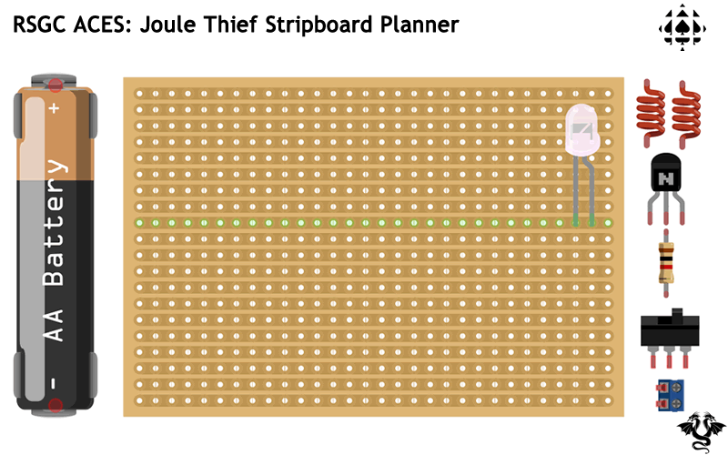
- Review this Electronics Club Primer on the use of Stripboard: https://electronicsclub.info/stripboard.htm
- To imporove your chance of success, grab a pencil and plan out the placement of the parts using this Stripboard Planning Sheet. Your BPS ST1 Stripboard is 31 × 19 (strips).
- Transfer and solder your supplemental parts to the Stripboard provided (coils, terminal block)
- Connect a AA alkaline battery to the circuit for testing (0.7-0.9 DCV works best).
- If it functions as expected, demonstrate it to Mr. D. to receive the 2-position Terminal Block to solder in, facing outwards.
- If it still works, present it to Mr. D. to receive your Keystone #2461 AA battery holder.
- Add a supplemental section to your DER and take a bow.
DER Task
 All ACES are required to undertake the first 5 Stages described above. Be sure to take great photos to supplement your DER presentation.
- Open your DER and make sure ALL the edits and corrections to your previous report are completed.
- At the end of your first report insert a Page Break to ensure this report (and all subsequent reports) start at the top of a new page.
- Add the project title, Project 1.2 Joule Thief, in Heading 1 Style
- Include the standard subheadings (Purpose, Reference, Procedure, Media, and Reflection) in Heading 2 Style
- Do as much research and mental processing as required to gain a good understanding of inductance, in general, and the operation of the Joule Thief circuit, in particular, BEFORE you start writing your Procedure. This MUST be in your own words. As I said in class, I've read thousands of DER in the past and I know when a student has written the text and when he has not. If I suspect the words are not yours I will simply reduce your credit.
- Since it has been awhile since your first submission, wise ACES will review the requirements for both the content and formatting of your DER
- Marks for this project will be awarded in multiples of 5, as in 0, 45, 50, 55, ..., 90, 95, or, possibly, 100.
- Be SURE to update your Table of Contents just prior to submitting your Report.
Additional...
MakeZine: Joule Thief
White LED Drive Circuit
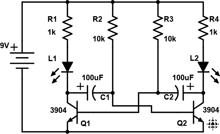
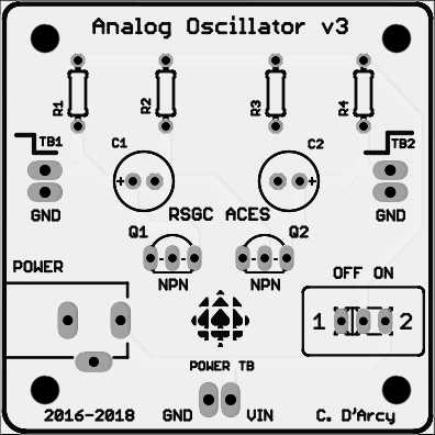
Project 1.2 Analog Oscillator
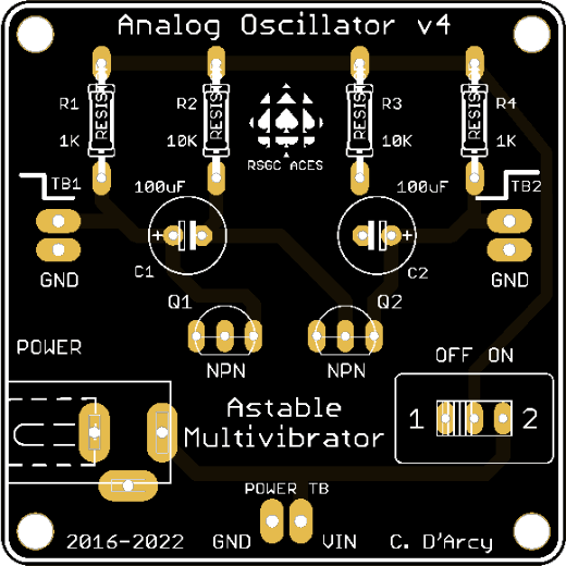 The square wave, a highly orchestrated sequence of alternating high and low durations, is the backbone of modern, digital, communication. The purpose of this project is to introduce you to the transistor and to demonstrate how it can be combined with other familiar analog components to produce an oscillating signal with properties similar to the digital square wave.
Task.
- Clean the lens of your phone's camera, as you will be gathering media (photos and videos) throughout this project, from start to finish, in support of your DER project summary due Saturday November 25.
- This project will test your organizational abilities as much as your nascent electronics' knowledge and skills. Part of the task includes thinking deeply about what you're doing.
- After studying the schematic of the Analog Oscillator (below, left) undertake your prototype (aka, blinker, Astable Multivibrator) on your breadboard. When you are confident the circuit has a chance of functioning, apply 9V power. Debug as necessary and document the results with your phone's camera.
You may wish to experiment with the rate at which the LEDs are flashing by adjusting the sizes of the resistors and/or capacitors.
| Analog Oscillator Schematic |
PCB: Dry Fit |
 |
 |
 Once you have obtained your media, you can request the additional parts that include a printed circuit board (PCB) and three terminal blocks. Disassemble your prototype and 'dry fit' the parts on your PCB (above right) in a manner similar to the image to the right (click to enlarge). This is an important step to appreciate the full scope of the task that lies ahead and to avoid the risk of soldering parts incorrectly that can be difficult, or near impossible, to repair.
- With your soldering area fully equipped with easy access to the required tools and conscious of the soldering techniques and strategies discussed in class and in this soldering video, you may begin the soldering stage. Remember,
- Never solder with the power to your PCB plugged in.
- Your soldering station should be kept no higher than 300°C.
- Keep the parts as tight to the surface of the PCB as possible. The reverse tweezers can help with this.
- The soldering tip should be clean and tinned.
- Any longer than 4 s with the soldering tip on the lead of a component runs the risk of damaging the part.
- Solder the smaller components first: resistors, then transistors, capacitors, slide switch then, finally the terminal blocks, ensuring they face outwards to permit LED lead access to the screw terminals.
- On multi-legged semiconductors, it is good practice to solder one leg, solder another part, then return to the original part. This practice minimizes the cumulative heat effect on parts.
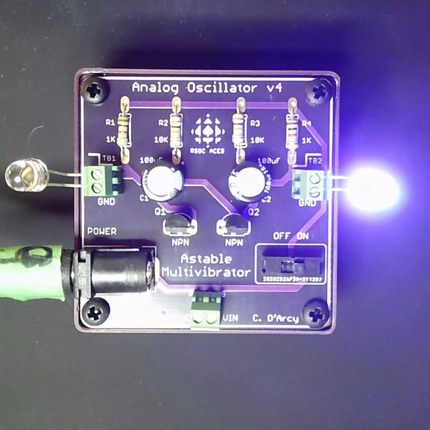 If you have invested care and thought into your efforts, plugging your 9V adapter into a temporary DC Power Jack should yield the desired outcome: a pair of blinking LEDS. If it doesn't function as expected, prepare yourself for the best part: debugging. Seriously, few activities are as satisfying as analyzing and repairing a faulty system. Use the large illuminated magnifying glass to check all your solder joints. Confirm your polarized parts are in the correct way. Use the DMM to to perform continuity, voltage, and integrity inspections. You WILL find the problem without the need to ask for my intervention.
- Once everything is as it should, present a working circuit to Mr. D. to get your Power Jack. Assemble it as you did for your Capacitor Visualizer.
- Finally, present both for your Analog Oscillator case and screws for final assembly.
- DER. Starting on a new page, add the Project name and complete sections under the subheadings: Theory, Purpose, Reference, Procedure, Media, and Reflection. Text is developed in accordance with the recommendations for Technical Writing and reflective of your much-improved formatting abilities. Graphic manipulation is undertaken according to the specifications laid out in the Engineering Report General Guidelines.
- Attach your DER to an email to ACEShandin@rsgc.on.ca with the Subject: Analog Oscillator by the deadline.
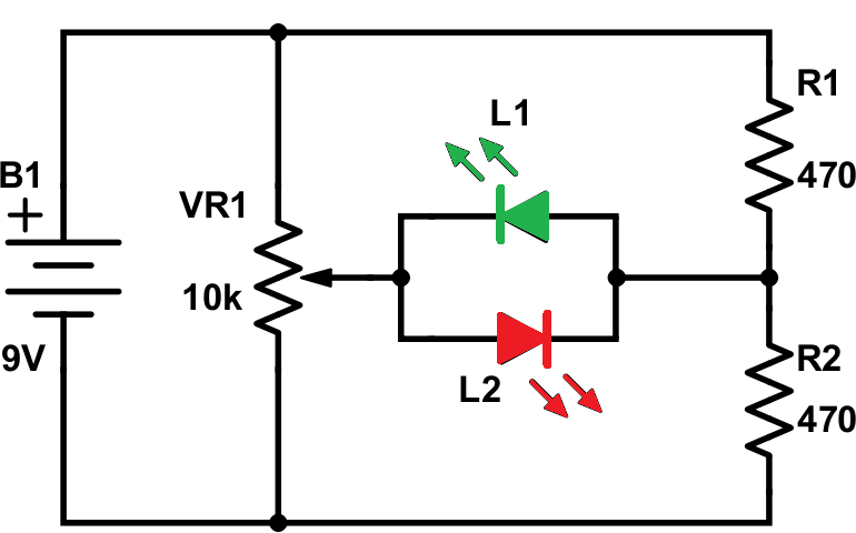
Project 1.? ACES Knight Light (Deluxe)
Below is the objective you're aiming for, in your first formal Design Engineering Report (DER) project. Ambitious? Certainly. RSGC's ACES program combines careful engineering and design elements to emulate a more complete prototype development experience. So, if you listen attentively to class instruction, employ strong organization and time-management skills this week and THNK, THINK, THINK, you will accomplish a goal you will be justifiably proud of. The project description appears below.
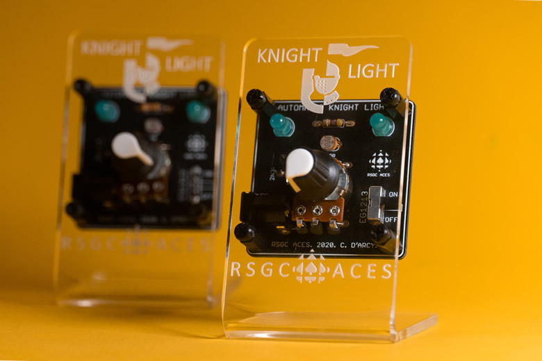
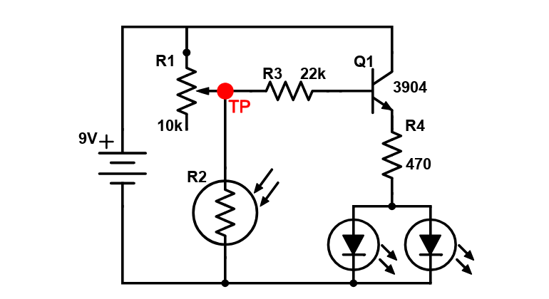 Class time has been devoted to the introduction of a number of analog components and provided you with an opportunity to develop a breadboard prototype of the ACES Knight Light circuit outline in the schematic to the right (click to enlarge). Heeding the advice and techniques described, develop a high-quality breadboard of the ACES Knight Light. Be sure to document your build using photos and video captured on your phone for later use in your Report.
- Following the detailed instructions and parts provided by Mr. D, prepare your 10 KΩ (panel mount) potentiometer for eventual use in your acrylic stand. Test the integrity of your soldering skills by replacing your blue breadboard trim pot with your panel mount version to confirm the circuit still functions as before.
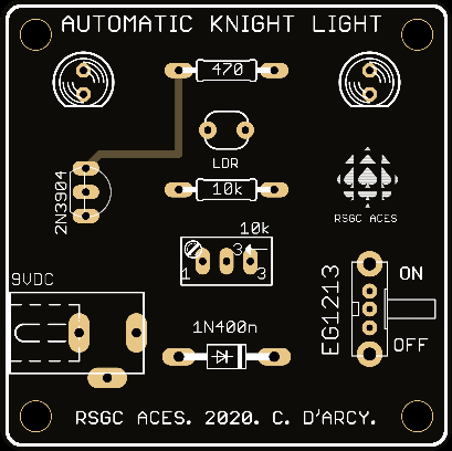
- Having listened and observed attentively to Mr. D's soldering demonstration, and reviewed the excellent soldering video prepared for you by a former ACE (N. Vassos), begin to transfer both YOUR parts and the SUPPLEMNTAL parts provided to you, to your custom ACES Automatic Knight Light PCB. Be sure to examine each solder joint carefully as you go, using the magnifying glass on Mr. D's desk if you need to. Have a DMM handy to confirm continuity and identify unintended shorts between leads every step of the way. Again, the best DERs are from authors who had their phone out capturing photos and video footage of the soldering process.
- Finally, solder your panel mount potentiometer to the PCB, making sure the three wires are an appropriate length. Attach your 9V battery. Test thoroughly.
- When Step 4 is complete, present your assembly to Mr. D. for his review. If everything appears to be in good working order he will provide you with the additional parts required to mount your PCB on the acrylic stand.
DER Task. Your writeup for this first project will include,
 Create the Word document, DER.docx that includes a Title page, Table of Contents (ToC) and headers and footers as discussed and developed in class.
- Each Project writeup in your ACES career starts on a new page.
- For this first project, start a new page after your ToC, be sure the page numbering starts at page (Arabic) 1, and place Project 1.1 ACES Knight Light in Heading 1 Style at the top of the page. Subsections, styled as Heading 2, must include,
- Purpose one or two short, well-constructed sentences that underscore the precise concept(s) being highlighted in his project
- Reference Include a hyperlink pointing to the URL of this project description and any other online resource(s) you explored with advantage
- Theory. Discuss the concept of a voltage divider in general, how it is employed in this circuit, what purpose it serves, and how the entire circuit works.
- Procedure You may use the schematic above right as long as it is properly sized or create your own. There are many options for this including:.Digikey's Scheme-It, Fritzing, Falstad, CircuitIO, etc. With specific reference to the Test Point (TP), marked on the schematic with a red dot, explain, using your new vocabulary, how the voltage at the TP influences the function of the 2N3904 NPN transistor. Include a complete, 2-column (asymmetric column widths), 3" wide, background-shaded, right aligned, Parts Table.
- Again, your Procedure discussion must be supported with a schematic that is, 3" wide, right-aligned on the page, and top-aligned with a paragraph.
- Media. Insert insanely clear, close range photos (can I distinctly see the colour bands of your resistors?) of your breadboard prototype, the front and back of your soldered PCB and the final masterpiece. Listen to my verbal comments of the best places and techniques for inserting photos into your report. Create a 2-minute video of your circuit with accompanying explanations and annotations of the components. Upload to YouTube within your own personal channel (not RSGC's) and include a full URL link in the Media section. Some of our best videos appear on our ACES' home page carousel. You can't afford to lose this video work.
- Reflection this is the only segment written in the first person and includes any comments you have about the concepts, the build process, any challenges you overcame and personal time-management issues you were pleased with or need to address in the future.
- Technical writing is done on the present, active voice, NOT presented in the first, second or third person. See these do and don't examples.
- Update your Table of Contents.
- Submit your DER.docx as
an attachment to an email to ACESHandin with the Subject Line: ACES Knight Light
Remember, your text should be developed in accordance with the recommendations for Technical Writing. Good luck.
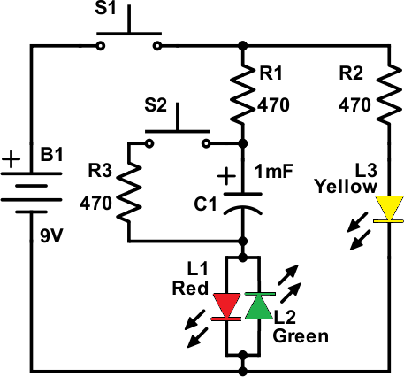
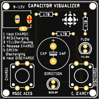
Project 1.1 Capacitor Visualizer
 Along with resistors, capacitors belong to a family of components known as passives in that they do not introduce a new source of energy into a circuit. Capacitors serve a number of useful functions in both DC and AC circuits. In completing this project you will strengthen your understanding that the capacitor (in series with a resistor), plays in the timing aspects of analog DC circuitry.
This project takes time to undertake properly, so be patient, and start early.
The schematic, below left, is of a straightforward test circuit that, in my view, best illustrates of the functional behaviour of an electrolytic capacitor in a DC circuit. You are familiar with the concept of a voltage divider from your first project. Looking at the junction (node) between S1, R1 and R2, we introduce the notion of a current divider as the current splits into two branches due to their parallel configuration.
We have discussed the charging of an empty capacitor and the effect this has on the capacitor in terms of its resistance (in AC circuits this property is referred to as reactance). In a DC circuit, a single RC Time Constant, denoted τ, can be expressed simply as,
`τ=R×C`
where τ is measured in seconds, R is measured in Ω, and C is measured in F. Also discussed in class (p. 33) is the expectation that after 5 RC time constants the capacitor is virtually fully charged (5τ~99%). One of the objectives of this project is to observe and confirm the expected results.
Tasks.
- To achieve the best results for each of the numerous trials, the capacitor should be fully drained. In the Procedure section of your report, explain how this is achieved in the circuit to the right.
- On a breadboard, prototype the circuit above left as neatly as you can using the first pair of resistor-capacitor values in the table below. Connect the longer lead of the bicolor LED to the capacitor and the shorter lead to ground. This ensures the orientation that agrees with the schematic. Note: Be sure to drain the capacitor and measure the voltage with your DMM to be sure. Explain this step in your Procedure and explain any related issues you have in achieving this.
- Once connected, hold the momentary button down (for as is required) before releasing it. Note the behaviour of the LEDs in particular, and try to explain what electrical behaviour at work, throughout. Do this a number of times until you feel you understand the principles.
- Now, more formally, using the timer on your phone, and through observation, record the approximate charging time for a fully discharged state until your eyes can no longer detect a visible state change in the red LED. A DMM can be used for more accurate results. Perform at least three trials with the first Resistor-Capacitor pair and record the average.
- For your DER, you are asked to duplicate the table that appears below. In the third column determine and enter the theoretical (expected) time to fill. In the fourth column, enter your observed result.
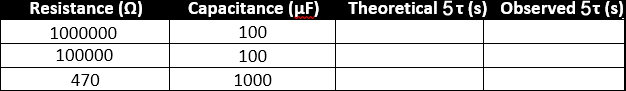
- Repeat Steps 3 and 4 for each of the remaining 2 RC pairs in the table. Again, perform a number of trials with each pair and record the average.
- For your DER summary of this Project, you MUST remember to obtain media of your prototype (both still images and video), before you dismantle it to solder together your completed device on the PCB provided. Be sure to watch the Instructional video, prior to soldering. Finally, demonstrate a WORKING version of your soldered PCB to me by Thursday October 31 to obtain a custom case for your device.
- In your DER, be sure to include the required sections listed above. You are to provide your own schematic using whatever aplication your prefer. It is up to you to decide the supporting images and graphics that engage your readers and leave them with a solid understanding of the concepts. The table above is large enough to be center-aligned on your page.
- Attach your (corrected) DER to an email to handin under the Subject Line: Capacitor Visualizer by the deadline.
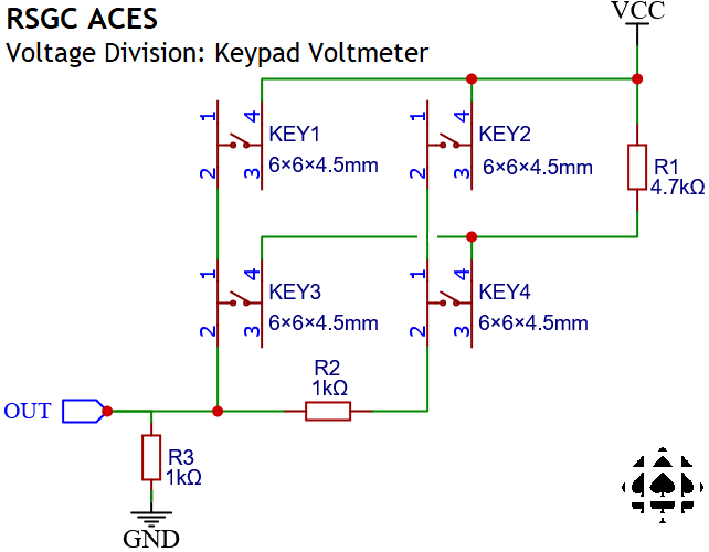
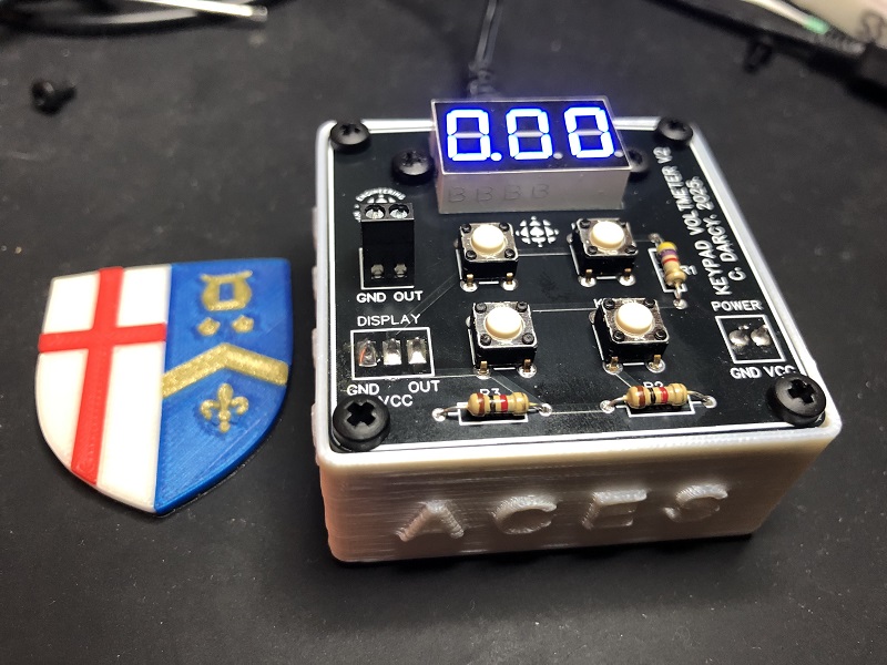
 Project 1.1 Voltage Division: Keypad Voltmeter
 This is the most complex first project ever assigned to an ACES Grade 10 class. If you LISTEN carefully, never simply guess and remain FOCUSED you will project will be a SUCCESS. If you miss classes, are disorganized, distracted or exhibit poor time-management you will come up short. It's completely on you.
In this project you are asked to investigate one of the many contributions to physics that Gustav Robert Kirchhoff made. His second circuit law, known as Kirchhoff's Voltage Law (KVL), has been one of the focal points of your first month in this course. This Law is a natural consequence of the Conservation of Energy principle in which states, that the sum of the voltages around a closed loop must be equal to zero.
Over the past few weeks you have assembled various circuits and confirmed through the use of your Digital Multimeter (DMM) support for KVL (the total of the positive supply (battery) voltage and the sum of the voltage drops across each component (negative) is zero)
ACES' reports earning the highest credit will prioritize these features,
- a detailed explanation of KVL, in text and images (photos, graphics) in the context of the three circuits presented in the task below. Well-composed photos of your DMM showing the voltage drops are encouraged. Your own custom schematics (See EasyEDA, Circuit Diagram, Falstad). Note. You are not to remove DMMs from the DES. Photos are to be taken in our lab.
- circuit prototypes with high build quality using the recommendations well-covered in our classes, and,
- high-degree of adherence to formatting conventions stressed in our four Word classes and itemized in our DER Guidelines page.
- a degree of creativity that separates your submission from the herd.
 Tasks (There are 7 Steps in all and each one must be done correctly before moving to the next, otherwise your project will be incomplete)
1. Examine the Keypad Voltmeter Schematic to the right, carefully (click to enlarge). Once you confirm your exact VCC supply voltage (iT is likely not exactly 9V), use your knowledge of Voltage Division to determine the value of the voltage that presents itself at the OUT node for the following situations. Record your calculations for your DER.
- When no key (button) is pressed
- When the single KEY1 is pressed
- When the single KEY2 is pressed
- When the single KEY3 is pressed
- When the single KEY4 is pressed
2. Prototype this circuit on your breadboard(s) as NEATLY as possible as photos will be taken for your DER. Confirm your determinations in Step 1 with a DMM. Correct your calculations if necessary.
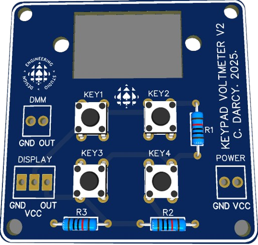 3. When your calculations are in order you will receive a PCB as shown to the right. From your toolkit obtain and NEATLY solder four momentary push buttons, two 1 kΩ fixed resistors and one 4.7 kΩ fixed resistor.
4. PAY CLOSE ATTENTION TO THESE INSTRUCTIONS AS THERE ARE NO REPLACEMENT PARTS. Present the soldered PCB to Mr. D'Arcy for inspection. If passed, you will receive the three terminal blocks. The two 2-position terminal blocks require their two small plastic post snipped off with your side cutters. Carefully solder the DMM block on the bottom because it needs to be accessible from the top. The POWER terminal block must be accessible from the bottom with the large jaws facing upward, so solder it on the top. The 3-POSITION DISPLAY terminal also needs to be accessible from the bottom so solder it also on the top with the large jaws facing upward.
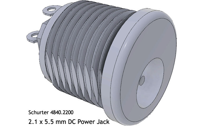
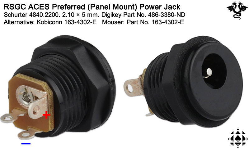
5. AT THIS STAGE YOU NEED TO CONFIRM YOUR PCK IS FUNCTIONAL IN ORDER TO COMPLETE THE FINAL STAGES.. Secure a 9 V power supply to the POWER terminal block from your breadboard. Secure wires from your DMM terminal block to a DMM. Press the respective buttons to confirm your calculations from Step 1 ans 2 above. Call Mr. D'Arcy to your desk when your results are successful. If so, you will be given a Schurter Power Jack as shown below, left. Solder 5 cm lengths of red and blue 22 AWG wire to the power jack as shown in the photo bottom right. Secure these wires to the POWER terminal block, apply 9V and test.
 |
 |
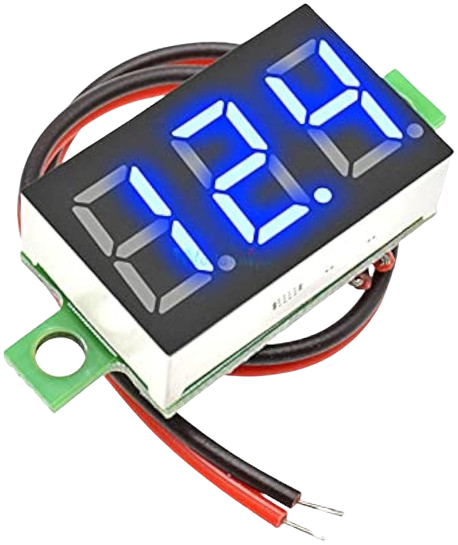
6. Present your powered PCB to Mr. D'Arcy for confirmation. If it functions as expected you will receive the Voltmeter, two additional M3 8 mm screws and nuts. The Voltmeter is installed from the bottom through the rectangular opening in the PCB. The screws go in from the top and the nuts secure them on the bottom. The three wires go to the 3-position terminal block as follows: red (VCC) black (GND) and white (OUT).
7. Present to Mr. D'Arcy for inspection. If it works, congratulations. You will receive your case and four M3 5 mm screws.
Finally, since this is your first DER submission, the graphic provides guidance on how to present your two Parts Tables for this project. Note: you are to recreate these tables in Word, not simply as graphics ripped from this image!!

Project 1.? Voltage H-Bridge
One of the most important skills an Engineer must possess is the ability to communicate, both in spoken word and in written form, in a highly structured format. Developing this skill takes much practice and this is precisely why your DER (Design Engineering Report) plays such a crucial role in our program, your mark, and your future.
 With the
  skills gained over the past few classes, you are ready to prepare your first DER submission. Furthermore, you are required to be familiar with the Guide for Technical Writing and, through practice and regular editing, your sentence structure will improve. Poor grammar and spelling skills detract from your presentation.
The Voltage H-Bridge circuit provides a vivid reflection of the fundamental voltage, current and resistance concepts we explored and analyzed over the first dozen classes. A schematic of the circuit appears to the right. The letter H is clearly visible in the depiction as the crossbar spans two voltage dividers (one variable and the other, fixed).
Task
- Create the Word document, DER.docx that includes a Title page, Table of Contents and headers and footers as discussed and developed in class.
- Each Project writeup in your DER starts on a new page.
- For this project, at the start of the first page following your Table of Contents (ToC), place Project 1.1 Voltage H-Bridge in Heading 1 Style at the top of the page. Subsections, styled as Heading 2, must include,
- Purpose one or two short, well-constructed sentences that underscore the precise concept(s) being highlighted in this project
- Reference include a hyperlink pointing to the URL of this project description and any other online resource(s) you explored with advantage
- Procedure discuss the concept of a voltage divider in general, how it is employed in this circuit, what purpose it serves, and how the entire circuit works. Finally, include a complete, 3" wide, background-shaded, Parts Table, and YOUR unique duplication of the schematic above right, created in Fritzing or some other schematic drawing application, 3" wide and right-aligned.
- Media formatted and captioned photos and (no more than) 2 minute video uploaded from your personal YouTube channel.
- Reflection this is the only segment written in the first person and includes any comments you have about the concepts, the build process, any challenges you overcame and personal time-management issues you were pleased with or need to address in the future.
- Technical writing is developed in the present, active voice, NOT presented in the first, second or third person. See these do and don't examples.
- Try to develop your OWN schematic images for inclusion in your submission and locate it appropriately in your Report.
- Create a short (1-2 minute) video of your circuit with accompanying explanations and annotations of the components. Upload to YouTube within your own personal channel (not RSGC's) and include a full URL link in the Media section. Some of our best videos appear on our ACES' home page carousel.
- Update your Table of Contents.
- Attach your Design Engineering Report (DER.docx) to an
email to handin with the Subject: Voltage H-Bridge by
the required deadline.
Remember, your text should be developed in accordance with the recommendations for Technical Writing.
(Optional)Task (for the Inspired)
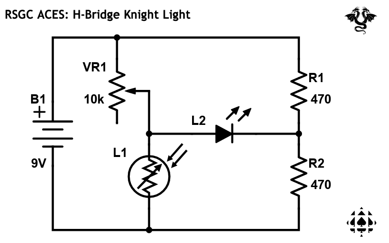 Highly-motivated students are encouraged to explore this related circuit based on the concepts of the Voltage H-Bridge.
- Examine the schematic to the right. Click to enlarge.
- The H-Bridge consists of two voltage dividers spanned by a standard LED.
- The voltage divider on the right presents a fixed voltage reference for the cathode lead of the LED.
- The voltage divider on the left is variable, through mechanical meads (pot) and optical influence (LDR)
- After thinking about why this can aptly be called a (K)night Light, breadboard the circuit and run a few tests. The cap of a Sharpie over the LDR does a good job of blocking the incident light.
- Add a summary of this extra circuit to your DER within Project 1.1.
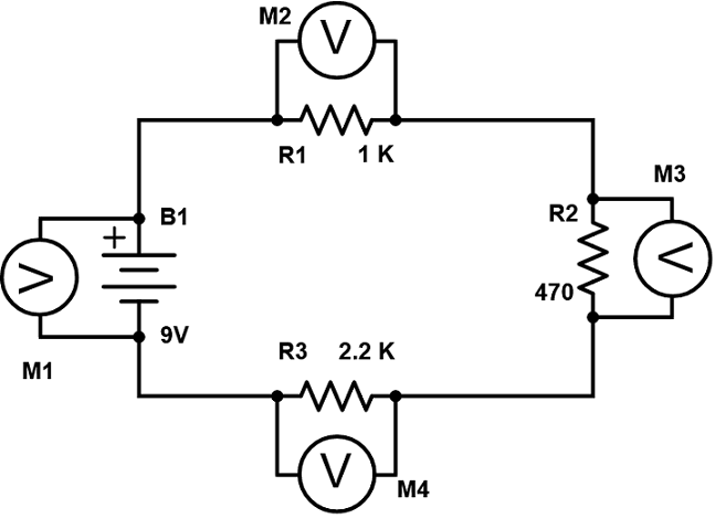
Project 1.? Kirchhoff's Voltage Law (KVL)
One of the most important skills an Engineer must possess is the ability to communicate, both in spoken word and in written form, in a structured format. Developing this skill takes much practice and this is precisely why your Design Engineering Report (DER) plays such a crucial role in our program, your mark, and your future.
With the skills gained over the past few classes, you are ready to prepare your first DER submission. Furthermore, you are required to be familiar with the Guide for Technical Writing and, through practice and regular editing, your sentence structure will improve. Poor grammar and spelling skills detract from your presentation as does content that I deem to be in words other than your own.
In this project you are asked to summarize one of the many contributions to physics that Gustav Robert Kirchhoff made. His second circuit law, known as Kirchhoff's Voltage Law (KVL), has been one of the focal points of your first month in this course. This law is a natural consequence of the Conservation of Energy principle in which states, that the sum of the voltages around a closed loop must be equal to zero.
Over the past few weeks you have assembled various circuits and confirmed through the use of your Digital Multimeter (DMM) support for KVL (the total of the positive supply (battery) voltage and the sum of the voltage drops across each component (negative) is zero)
ACES' reports earning the highest credit will prioritize these features,
- a detailed explanation of KVL, in text and images (photos, graphics) in the context of the three circuits presented in the task below. Well-composed photos of your DMM showing the voltage drops are encouraged. Your own custom schematics (See EasyEDA, Circuit Diagram, Falstad). Note. You are not to remove DMMs from the DES. Photos are to be taken in our lab.
- circuit prototypes with high build quality using the recommendations well-covered in our classes, and,
- high-degree of adherence to formatting conventions stressed in our four Word classes and itemized in our DER Guidelines page.
- a degree of creativity that separates your submission from the herd.
Note 1. Through your additional research you will come across some heavy mathematical models used to support KVL. You are to skip this in Grade 10, postponing it until your university years.
Note 2. The task described below is purposely short on detail. Rather than provide a laundry list of elements you must include, I prefer to have my students show me what they feel are the most important elements to include. In this way I get to know each of you better.
Note 3. The credit earned for this first submission will be limited to a whole number out of 10 (0, 1, 2, 3, ... 7, 8, 9)
Task.
- Review, one more time, the structure of every Project Report in a DER that appears at the top of this page.
- After extensive research, thinking and breadboard prototyping attempts, you are to present THREE circuits (the two circuits below and one of your own choosing) in terms of Kirchhoff's Voltage Law (KVL). This would include an explanation and supporting images of your prototypes confirming the voltage drops across the major components in the context of KVL.
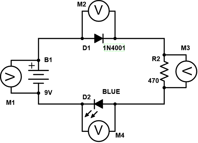
- In your Circuit 2 explanation, include a discussion of the purpose and role played by the 1N4001 power diode.
| Circuit 1. Three Fixed Resistors |
Circuit 2. Diode, Fixed Resistor, Blue LED |
 |
 |
- Update your Table of Contents.
- Attach your Design Engineering Report (DER.docx) to an
email to ACESHandin with the Subject: Kirchhoff's Voltage Law by
the required deadline.
Last Update: 2024 10 07


