
 Your exceptional CHUMP journey has prepared you for your next privilege: the deepest possible drilling into the hardware and software of modern microcontroller technology. The carefully designed sequence of mid-level coding exercises below, exploiting familiar ACES' optical devices, is the final preparation for Session 5: Pure Assembly Language Programming of the AVR ATtiny84 on the Dolgin Development Platform (DDP), in 2021.
Although these C coding exercises can be considered high-level, they call for a deeper understanding of the underlying architecture of the AVR family of MCUs, in particular, the ATtiny84. Hence, I refer to this coding as mid-level. The magic behind function such as pinMode(), digitalWrite(), digitalRead(), and shiftOut() for example, are exposed and rewritten, in some cases, more efficiently. Direct port bit manipulation of the MCUs' General Purpose Input/Output (GPIO) Registers are called for to achieve improved performance. Conveniently, your CHUMP experience has given you the necessary insights that were lacking at the end of Grade 11 to guide these next steps.
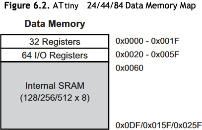
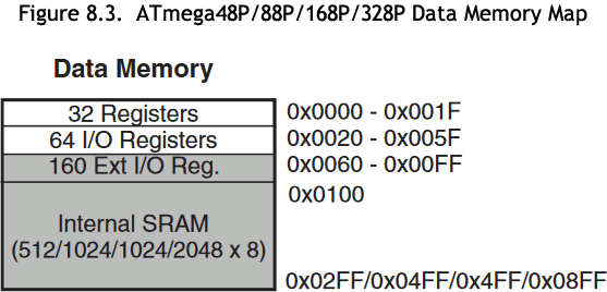
The graphic to the right is the general layout of SRAM on the ATtiny84. Compare that to the SRAM of the ATmega328P. Similar.
The exercises on this page are to be undertaken on a breadboard ATtiny84 hardware platform you are required to construct (see below). Although this tutorial from MIT's 2014 High-Low Tech group on the virtues of the AVR tiny family is showing its age, it is worth reviewing, as a starter.
The AVR ATtiny84
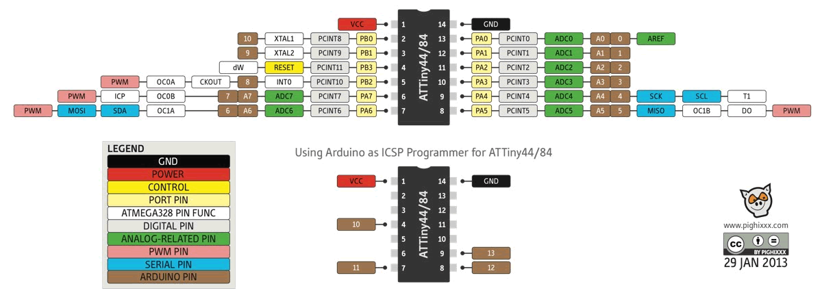
The pinout diagram below will facilitate your build. The correlation between hardware pin numbers and the software pin numbers is highlighted in Brown.
Finally, familiarize yourself with these C header files that are #included, by default, into the Arduino IDE's Toolchain, based on the target Board you select.
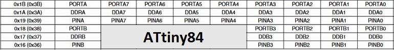
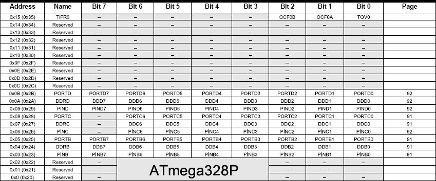
ATtiny84 GPIO Register Reference
ATtiny84 Register-Level Exercises
You may wish to create a folder entitled RegisterLevelCoding or something along those lines, to house this unique set of sketches I am asking you to develop.
 1. General Purpose Input/Output (GPIO) Tests.
After days of preparation, I have settled on the Task below as your first experience with mid (or register) level coding.
Task.
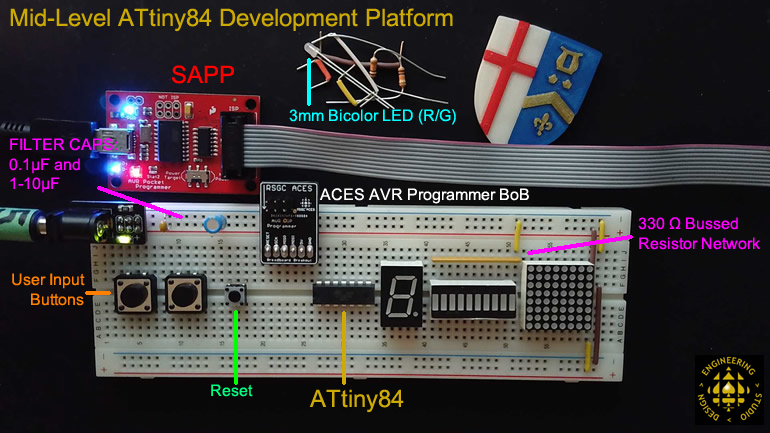
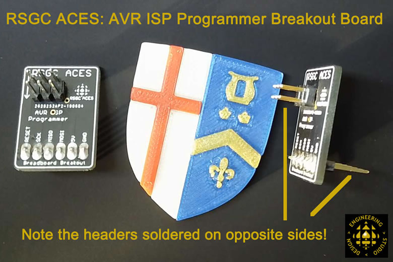 For the majority of next few months you'll be programming your ATtiny84 with your Sparkfun AVR Pocket Programmer (SAPP). Code is uploaded from the Arduino IDE through the Upload Using Programmer menu item within the Sketch menu (Ctrl+Shift+U). ISP connections with your ATtiny84 is accomplished with the support of the ACES AVR ISP Programmer BoB using the USBtinyISP (ATTinyCore) protocol selected with in the Tools>Programmer menu.
- Grab a free breadboard and assemble our Mid-Level ATtiny84 hardware platform modeled on the annotated photo below. The optical devices, from the 7-segment display to the right are not needed for this exercise. Your two 3mm bicolor LEDs in your loot bag, are. This layout, will, ultimately, provide a smooth transition to your Mid-Level Matrix Project due December 19th, or earlier.
- New MCUs directly from the factory are not quite compatible for breadboard use, in particular, their clock source. Select Tools>Burn Bootloader to set the correct clock source.
- In addition to configuring the clock source other features can be slected by setting parameters by fuses. Check out this useful AVR Fuse Calculator (link also found at the top of our course page)
- Be sure to wire the RESET pin with a 10 kΩ pull up resistor and a momentary button that creates a falling edge when pressed.
- Remember, this an MCU, so it's 5V, all the way!
- Create a new project called GPIOTests and drop in this code.
- This code is fully functional and we'll go though it, statement-by-statement. Your task is to comment each statement as to its purpose and/or function.
 3. Mid-Level ATtiny84 Makeover of the Classic I/O Functions
 This is a large pool we're wading into, so let's start in the shallow end. Some of the first Arduino functions you were introduced to were pinMode(), digitalWrite(), digitalRead(), and shiftOut(). Those simple blinking LEDs provided early, but important, confirmation that your software and hardware efforts were meshing, and on the right track. The only problem was that there was too much 'behind the curtain' magic that, over a year later, we need to explore in order to optimize our future engineering objectives.
Task.
- Review the other graphic assets provided on this page above to wire up your AVR Programming BoB and your ATtiny84. Use the silkscreen printing on the AVR ISP Programmer BoB to direct your six essential connections.
- Wire in the RESET function of the ATtiny84 in the same manner as you did your standalone ATmega328P last year, with a 10 kΩ pullup resistor to the small 5mm ground momentary button, shown.
- In keeping with the "Honey, I shrunk my MCU", your Session 4 loot bag contains a couple of 3mm bicolor LEDs (even LEDs are smaller from here on in). Place one of them so that it spans the ATtiny84's digital pins 9 and 10.
- Create a project called MidLevelFunctionEquivalents and drop in this shell.
- This is your first official sketch destined for the ATtiny84 so, within the Board Manager dialog, ensure you have the latest version of Spence Konde's ATtinyCore installed.
- You'll be using your Sparkfun AVR Pocket Programmer (SAPP) with your BoB for these exercises so make sure you have USBtinyISP (ATtinyCore) selected as your programmer.
- Under the Sketch menu, select Upload Using Programmer to flash this code shell. Debug as necessary.
- Now, examine the code. You need to write the bodies of the three functions, using direct references to the GPIO #defines (iotnx4.h) in order to the have the bicolor LED alternately flash red and green. To make the logical connection between what the new functions need to do, I've simply swapped the names, as follows: modePin() replaces pinMode(), writeDigital() replaces digitalWrite(). and readDigital() replaces digitalRead().
 4. First Look at Custom Libraries
 You've employed a number of libraries over the past year or so, from the Arduino Core libraries (automatically included in every project) to third party libraries (through the explicit use of the #include directive) that abstract the functionality of complex devices and tasks through convenient object instantiation and subsequent member function calls. Well, it's time to construct YOUR first custom library, containing the ATtiny84 functions from these practice exercises. In doing so, future projects can reuse this code to yield the desired outcomes in less time, and with improved confidence.
 Task 1. Separation of Code. First, identify code that is reusable and confirm that it can exist in a separate file.
- Open the previous project, MidLevelFunctionEquivalents, and save it as MidLevelFunctionLibrary.
- Click on the Down Arrow icon in the top right corner under the Serial Monitor icon, and select New Tab.
- Enter tn84Support.h in the text box and press OK.
- Cut the functions out of the primary file, click on the new tab, and paste them into the ACES_tn84.h file.
- Return to the primary file and, just under the opening comments, add the directive, #include "ACES_tn84.h". Be sure to use the double quotes which reference a header file within the same project.
- Compile (Verify) to confirm all your code remains reachable, despite being split into separate files.
- Upload and conform everything is functioning as before.
 Task 2. Centralized Access to Common Code. Now we can place the reusable code in a folder that is accessible to future projects!
- Close the Arduino IDE.
- Use the Finder to locate your personal Arduino sketch folder. Within this folder you have a libraries folder. This is where the Arduino IDE's Library Manager has previously stored libraries you have downloaded.
- Within this libraries folder, create a new folder called ACES_tn84.
- Go to the MidLevelFunctionLibrary project folder, remove the ACES_tn84.h file and paste it in the newly created ACES_tn84 folder.
- Now, reopen the Arduino IDE, and the MidLevelFunctionLibrary project. Notice the tab with the ACES_tn84.h file is no longer there.
- Open the Include Library feature within the Sketch menu, find the ACES_tn84 library, and select OK. You'll notice the directive, #include <ACES_tn84.h> has been inserted into your sketch. Notice the angle brackets (instead of the double quotes as before) to indicate the library is NOT within the same project.
- Upload the code. It should be good and you can now do the same for future projects.
- As you develop new features and functions you may wish to add these resources to the tn84Support.h file.
- See? !!
- From here on in, consider adding resources to your ACES_tn84.h library , and other custom libraries to accelerate your project development timelines. Remember, ACES are committed to efficiency, accuracy, and high productivity. This world needs engineers that bring all three.
These are some of the familiar ACES optical devices we'll apply our nascent mid-level coding practices to ...
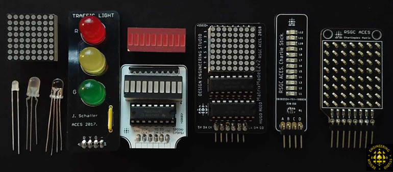
 5. 3mm Red/Green Bicolor LED.
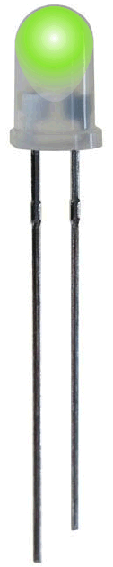
Your Session 4 loot bag includes two 3mm bicolor LEDs (red/green). Place its two leads in PA6-7, with the longer lead in PA6.
Create the project BicolorAlternation that employs direct, register-level GPIO Port manipulation resulting in red/green alternate flashing every half second.
 6. PlayByte. 5mm Red/Blue Bicolor LED.
 Your Session 4 loot bag also includes a 5mm bicolor LED (red/blue). Place its three leads in PA0-2, with the second longest lead in PA0.
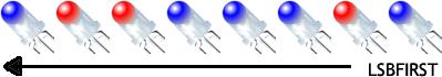
Create the project PlayByte that employs direct, register-level GPIO Port manipulation resulting in a continuous, 8-frame animated sequence that 'plays' a byte in an LSBFIRST order. The code is to be Red for 0 and Blue for 1. Each colour is to be held for 1 second, with no delay or gap in between. At the end of the 8-bit colour sequence, turn the LEDs off for 3 seconds before repeating, indefinitely.
Example. The image (above right) reflects the playing of B10011101 (or 0x9D or 0235 or 157).
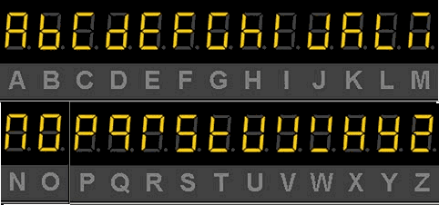
7. ASCII Alphabet on a 7-Segment Display.
 Your ICS3U experience introduced you to the concept of a segment map (array) for an ASCII letter lookup table (LuT). The code can be found at
  AVRFoundations: Write7SegUpperCaseCharacters.ino.
Obtain the array code for the segment map and drop it into a new project entitled ASCIIAlphabet. Develop register-level code that makes optimum use and efficiency of the ATtiny84's ports to continuously cycle through the LuT, displaying the letter representation on your 7-segment display device.
8. 10-LED Bargraph.
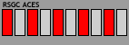 (The ATtiny84 is just that, tiny, so this exercise may push the limits of the MCUs GPIOs). Create the project BargraphAnimation that uses a 1:1 GPIO port pin to LED mapping to duplicate the animation depicted in the image to the right. Strive to make it as efficient as possible.
9. Register-Level 74HC595 Shiftout (Morland Bargraph).
 The previous exercise left little GPIO room for anything else. We need to drive a 10-LED bargraph with fewer port pins, so we return to the 74HC595 shift register. However, in this iteration, we forego the use of the core shiftOut() function in favour of our own register-level bit manipulation strategy.
First, review the primer below on the 75HC595.
Create the project ShiftOutAnimation that duplicates the result of the previous exercise but only requires three ATtiny84 GPIO pins, as opposed to ten.
10. 64-LED 2D Matrix.
11. ACES' CharlieStick. TBC.
 12. ACES CharlieMatrix. TBC.
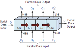 A shift register is a device typically used to expand the number of pins of a microcontroller. The most common design by far is based on the 74HC595 architecture. Using (as few as) three pins of the MCU (coloured) you are able to control 8 (or more) data lines (QA..QH). In addition to the three pins that control shifting, two other pins (Output Enable and Master Reset) provide additional (Active Low) control over the state of the 8-stage internal register set and output latches.
The IC accepts bits serially and presents them on output pins in parallel.
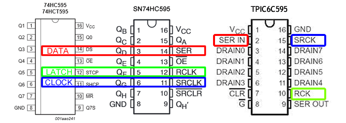
Two sets of naming conventions for pins tend to confuse those new to the IC. The image below tries to address this issue.
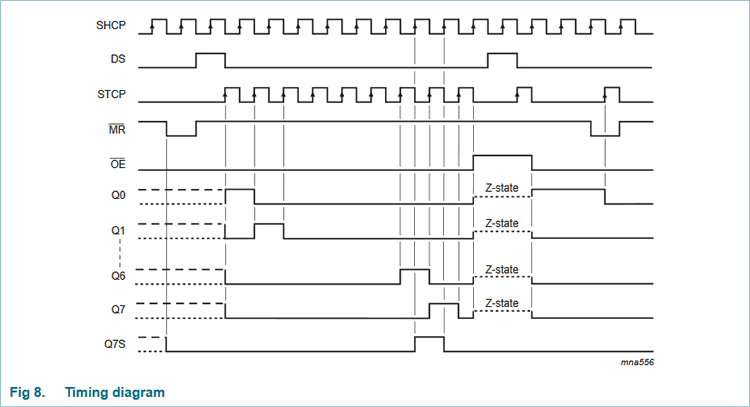
2. Waveform Timing Details. The digital orchestration of serial input bit stream is summarized in a waveform or timing diagram. A more detailed explanation of the mechanics of Serial to Parallel Shifting-Out with the 74HC595 can be found by following the link to the Arduino tutorial. Let's attempt to decipher the timing diagram, extracted from the 74HC595 datasheet,
As you are well aware, the immediate benefit of the Arduino shiftOut function is to hide the details of the digital dance allowing the higher-level programmer to concentrate on more macro concepts. However, hiding details always comes at a cost; if not performance then, at the least, in understanding. Our goal is to solidify our lower-level coding skills through direct handling of the signals on the three control pins, thereby bringing you closer to the AVR and IC hardware. This brings all sorts of future dividends.
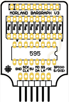
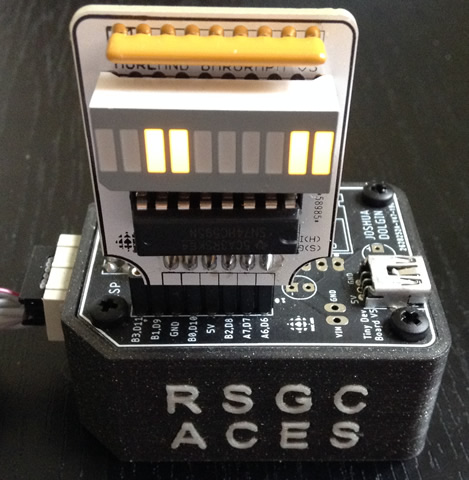 3. Prototyping Platform. Insert your Morland Bargraph into the DDP in the most feature-suitable position (supply and PWM) as shown to the right.
4. Register-Level shiftout. With the signals and waveforms of the 74HC595's timing diagram understood, we can now tackle the low-level responsibilities of the waveform ourselves through direct register manipulation. Remember, our goal is to enlighten, not suggest this is the preferred alternative in all cases.
- The function syntax we're going to simplify that conventional
shiftOut header function. We'll use a purely lowercase shiftout to avoid compiler confusion,
// LSBFIRST:0 MSBFIRST:1
void shiftout(uint8_t order, uint8_t value)
Complete the body of the function, hard-coding the port manipulation for this platform.
- Add code to your
loop() function that exercises your shiftout() function to display an interesting pattern on the bargraph.
- Questions worth considering: Where is the power coming from to drive the LEDs? Does it come directly from the MCU or does it come from the 595's output pins? What are the maximum voltage and current capabilities in either case?
Not surprisingly it's an important point that was answered pretty well on this forum...
