 Given that ACES is an acronym for Advanced Computer Engineering School it seems appropriate to introduce students to just that: building their own computer processor from scratch. As Ken Shirriff reminds us, "Before the microprocessor era, minicomputers built their processors from boards of individual chips." It is highly instructive for ACES to physically manipulate and explore this precise architecture prior to their undergrad years that will demand far less of you. Alan Kay's 1982 quote provides further inspiration, “People who are really serious about software should make their own hardware”.
Ben Eater has an exceptional blog that takes the viewer through the stages of building an 8-bit processor on a breadboard. Furthermore, his website offers the entire parts kit should one choose to take the plunge. As terrific as this is there are two glaring problems with this design for ACES. First, any 8-bit design imposes a time and cost premium of roughly double that of a 4-bit design. Even more problematic is that, Eater's resources are simply too good! As much as he decries the use of kits and PCBs that one simply follows instructions and solders parts to, leaving little struggle and growth for the prospective engineer, Eater's presentation borders on much the same. ACES need to engage a struggle while in high school if they are to grow, personally.
Back in 2010 I came across a pdf that provided the ideal foundation for our ACES needs and it addresses the two major shortcomings of Eater's 'paint-by-numbers' offering: A Simple and Affordable TTL Processor for the Classroom. D. Feinberg. The beauty of Feinberg's paper lies not within what he tells you, but rather, what he doesn't. You see, it is the gaps in his explanation that provide space for you to actively participate in the development and thereby earning ownership. By engaging these challenges, you gain insight, confidence, and earn a sense of deep satisfaction that you'll remember for a lifetime. So, here we go...
Reference: CHUMP Workbook
CHUMP Task Sequence
 You are about to embark on a hardware project that holds the promise of being one of the most important achievements to date of your young scholastic career, that is, to build a 4-bit computer from scratch. Reaching the summit will test your passion, dedication, and commitment to an engineering undergraduate program. D. Raymond and J. Corley accomplished the feat in their 2018/2019 ICS4U year:
 https://www.youtube.com/embed/vZ13xud0qBc
- Code. With reference to the CHUMP Instruction Set, develop and submit a unique and (somewhat) interesting CHUMP program (presented in the manner below) as your first DER entry in your CHUMP Report. Your goal will be to demonstrate that the program you write this week, will run on the processor you build six weeks from now.
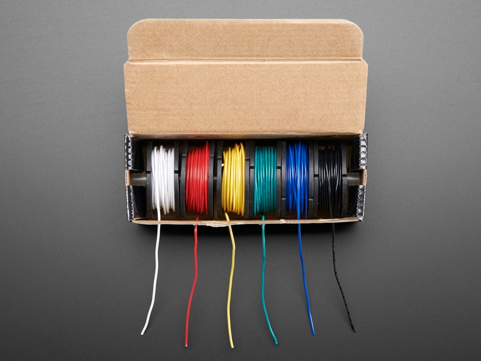
- Clock. Following Ben Eater's terrific 4-part video series on the 555-based Clock module, build, test and report on your own module. This will be the heartbeat of your CHUMP. For this project you MUST use the following parts I supply you with: Quad breadboard, 500 kΩ trim pot, rectangular LEDs (red, green, yellow), 3×555 timers, strip of 0.1μF caps, TTL AND, OR, NOT logic ICs, slide switch, and bags of 0.3" and 0.4" preformed jumper wires. Please take great care with these parts; they are not replaceable. Power can come from a 5V AC/DC adapter or your Arduino for the time being. Finally, for both your text and video presentations, strive to be as clear, concise, and detailed as Eater has been in his presentation, even going one better than him with a video that is under 3 minutes:)
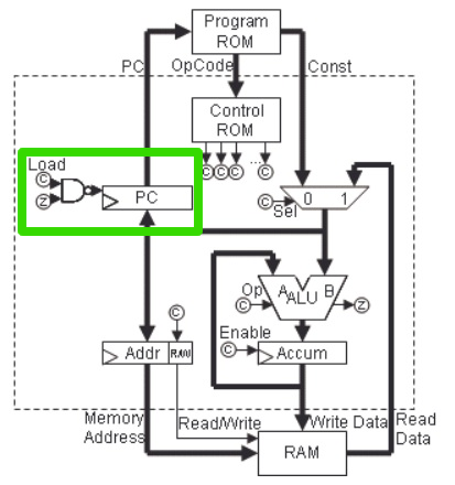 Program Counter. In this Stage, you are expected to complete your wiring to your clock, the SN74LS161 counter and the NAND logic to provide eventual support for the counter's LOAD feature. Four rectangular LEDs on the output pins of the Program Counter will confirm your counter is advancing on the RISING edge of the clock signal. So,
- Strip off any of your previous experimental builds, with the exception of the full Eater Clock build. Confirm this clock is still fully functional with an LED indicator. Do not proceed until this is working. Ok, good.
- Now, wire in your SN74LS161 counter and supporting NAND IC (SN74LS00), reading the strikingly lean notes on the IC provided in the CHUMP workbook. There is no need to invest a great deal of time cutting and stripping wires to exact lengths as there are so many steps ahead, the optimum location of the program counters can not be known at this point. Just ensure that wiring is neat and understandable. You may choose to attach a separate clock bus to your ABRA-48.
- Attach two buttons to your NAND IC with pull-down resistors. These buttons will simulate the as-yet-to-be implemented C and Z flags that will trigger a JUMP on the counter's /LOAD pin. To confirm correct functionality of this feature, wire a sample nibble on the SN74LS161 Input pins using the 4-position DIP switch with 1K pulldowns (any higher and TTL ICs struggle with too little current), and test.
- Place 4 tightly-arranged, easy to read, rectangular LEDs you were provided with (no resistors required) on the outputs of the SN74LS161 to confirm the counting, just as you did EXACTLY in Grade 10 with the 4510. Do not proceed until this is working.
- Confirm that the clock is advancing on the rising edge of the clock signal. If it isn't, determine what the problem might be and repair. Ok, good.
- Wire a pull up resistor to the /CLR pin of the SN74LS161 (pin 1). Integrate a momentary button to the /CLR function, enabling the operator to perform a temporary grounding of which, resulting in the clearing (0000) of the 4-bit counter.
- For this segment's accompanying video, demonstrate both the free-running and single-step clock features through full execution cycles of the program, as well as the /LOAD feature and /CLR features. Include a discussion of your build and placement decisions.
- Write the DEReport for this stage and submit.
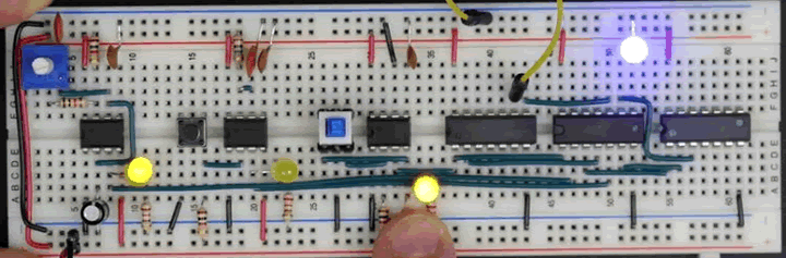
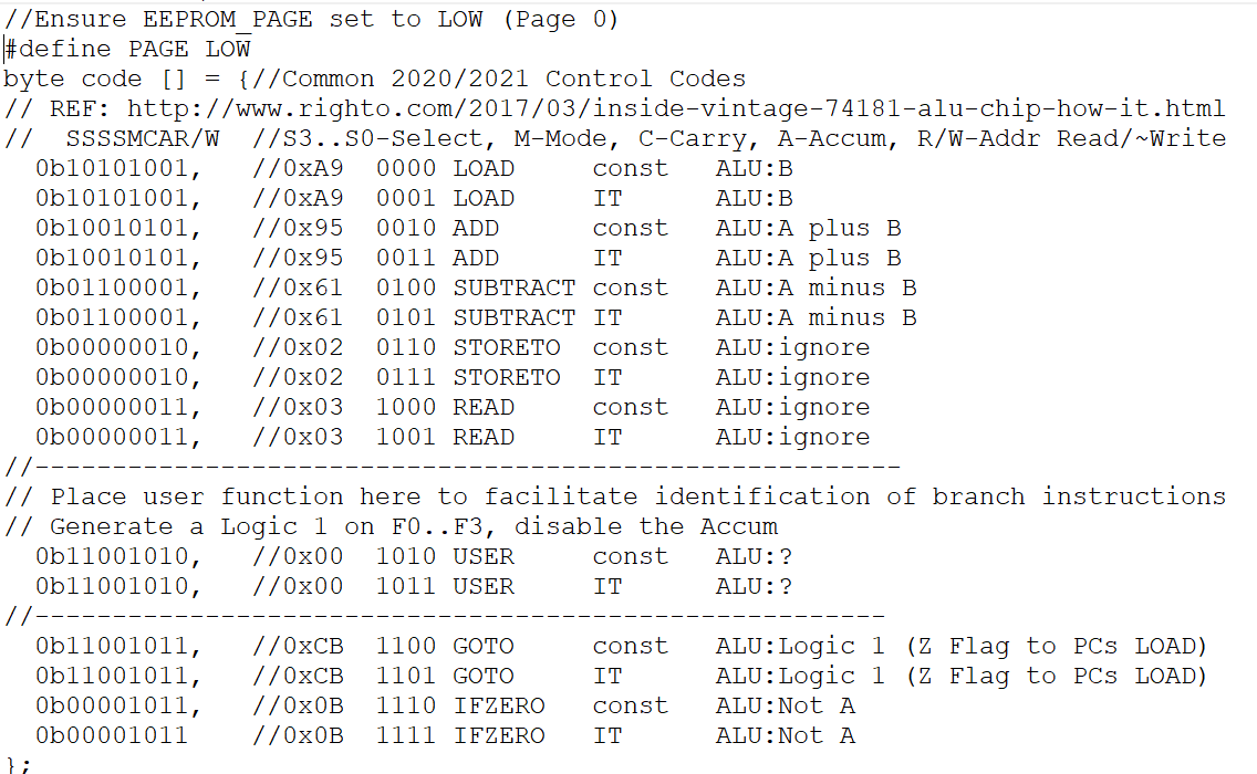
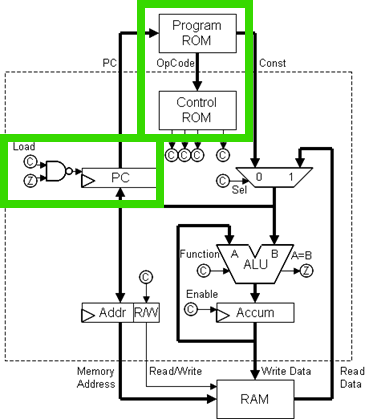 Program (and Control) EEPROM. In Stage 3.3.2 of your CHUMP build you will provide visual confirmation, either through rectangular LEDs or dual LED displays (see below), that both the machine language version of Feinberg's sample CHUMPanese code (Page 0) AND your custom code from the previous stage (Page 1) have been successfully flashed onto your AT28C16/AT28C17 Program EEPROM IC. Additionally, as a replacement for the complex combinational logic circuitry that would provide dynamic control for our processor's various modules and to provide storage for the machine language version of our program, we'll (eventually) need to flash a set of (as yet undiscussed) control codes on the second Control EEPROM.
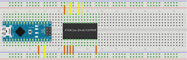
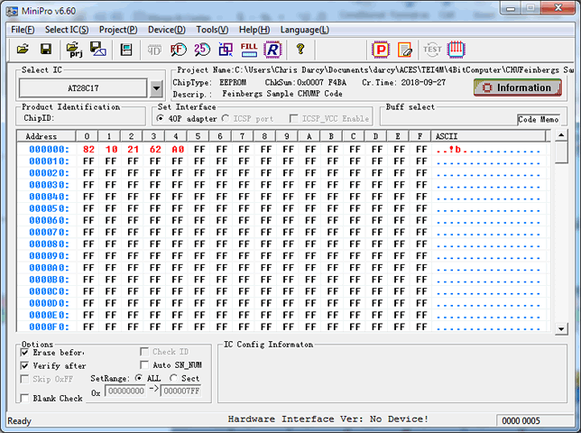
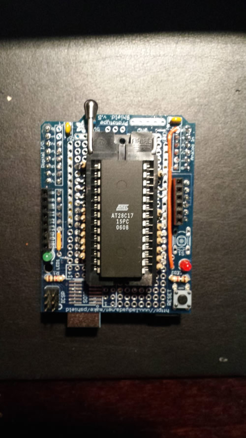
After viewing Eater's two (incredible) videos, wire your MCU of choice into an EEPROM on a breadboard (see below), create the programmer sketch (that uses an 8-bit integer array to hold the CHUMPanese code) and flash your code from 3.3.1 onto the AT28C16 EEPROM. Here's my version (echoes to a shift register/bargraph) that uses our UNO EEPROM Programmer Shield.
Now, once your Program EEPROM has been successfully flashed,
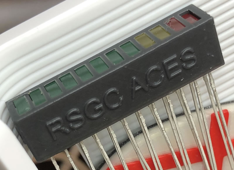
- wire your four SN74LS161 outputs to the A0-A3 address inputs of your Program EEPROM. I think you can figure out what to do with the three control pins (/WE. /OE, and /CE). Place the rectangular LEDs you were provided with (packed together in an ACES Bargraph holder) on the 8 I/O outputs of the EEPROM to confirm you're seeing the program that you've successfully flashed.
- For this segment's accompanying video, have a paper copy beside your partial processor that includes a table containing both your CHUMPANESE assembly code statements adjacent to their equivalent machine code instructions. Single step through the clock signal while discussing and confirming your instructions are accurately preseted on the LEDs.
- Think and implement something extra!
- Write the Report for this stage and submit.
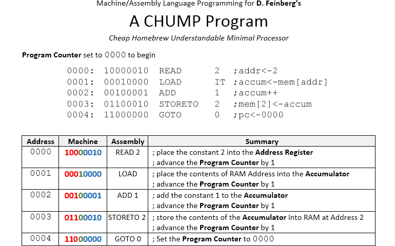
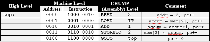
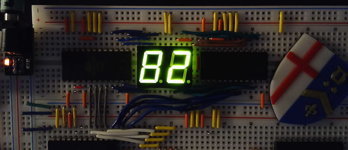
ACES' EEPROM Enhancement. A further interesting application of the EEPROM ICs is the support it can provide for a dual 7-segment display of the hexadecimal machine codes for your CHUMPanese program. Similar to the 4511 BCD decoder IC you used in the Grade 10 counting circuit, the EEPROMs replace the required combinational logic. In the image below (click for video) two AT28C16 EEPROMs (OP code and OPerand) were flashed with the same 16 single-digit maps of the digits from 0 to F. A ROHM LB-602MK2 dual display accepted the output from each of the EEPROMs. The video reflects the machine code from Feinberg's sample above: 82 10 21 62 A0...repeat
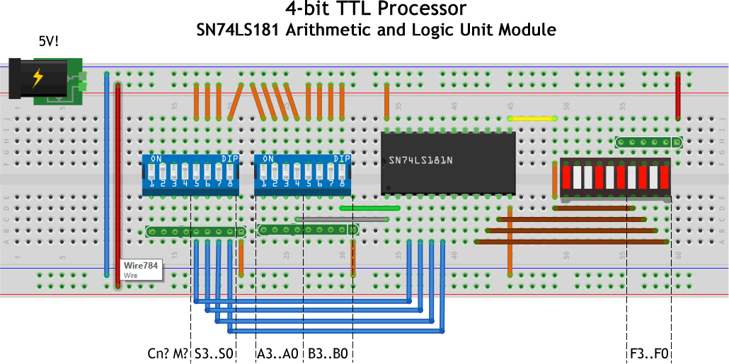
- Arithmetic and Logic Unit (ALU). Assemble, test, and report on the SN74LS181 ALU Module. This is one STRANGE IC as can be seen in these seemingly contradictory references. This stage represents the final independent exploratory module before we attempt to build our entire processor. Employing ACTIVE HIGH logic, wire up an ALU circuit that can be used to explore the 32 functions (16 logic and 16 arithmetic) the IC is capable of performing. For this submission only, arrange your circuit so that it closely matches the diagram below. (SN74LS181N.fzz) Note. Finally, make a sincere effort to lay out your board with care and consideration so that your ALU video is clear, informative, and compelling to view.
- To deepen your understanding of the SN74LS181's 16 Logic Functions you are asked to complete the remaining 15 tables in this worksheet and include them in your DER with this stage of your CHUMP Report.
- Since the A=B pin provides critical support for branching within your CHUMP code, be sure to include evidence in your video of activating this 'open collector' pin
- As well as an overview of the 74LS181 and its more common functions, your video should highlight the specific functions you will call upon in your custom CHUMPanese code.
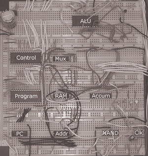
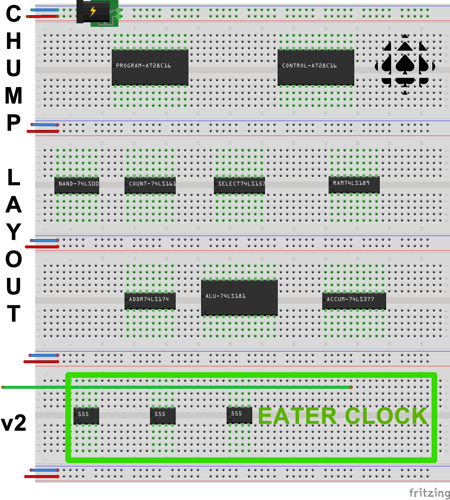 RAM, Mux, Address, Accumulator and Control EEPROM. Your next-to-last CHUMP stage pulls the last two months of development together. Here's the rough task sequence we'll follow,
- The RAM (74LS189), Mux (74LS157), Address (74LS174), Accumulator (74LS377) and EEPROM (AT28C16) Expert ACES must be ready to answer questions from the group as we navigate the development of the control codes.
- After a review of CHUMP's Address, Data and Control Buses we're ready to develop the contents of our Control EEPROM. See page 40.
- Dust off your EEPROM Burner and flash your Control EEPROM with the codes you've developed.
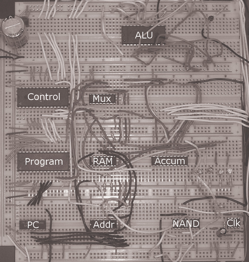
- This stage may require a significant rearrangment of the CHUMP ICs on your board as you introduce (potentially) the final set of ICs. A general outline of your CHUMP processor appears to the right.
- Wire in the remaining ICs. You are encouraged to use your wire kit to colour-code the Address, Data and Control Buses.
- Incorporate current limited LEDs (preferably rectangular, in custom ACES bargraphs) strategically, throughout your build for an enhanced view experience.
- For this segment's accompaying video, you are asked to lead off with exactly three full executions of your CHUMP code, at 1 Hz, so viewers (me) can witness the precise LED or 7-Segment representation of your machine language instructions. On the heels of that you can engage in a discussion of your build.
- Write the Report and submit.
 |
 |
- Code (Revisited). As is fitting, your CHUMP marathon concludes by revisting its starting point. Weeks ago you were asked to write software for a hardware device you had not constructed. In this final stage you asked to flash the code you commited to at the beginning of this project onto your Program EEPROM and demonstrate its execution on your processor. Include the code again in your DER, noting any minor modifications required to account for details you may have overlooked or had been unaware of. Be sure to include coverage of this executing software in your summary video.
- Congratulations on achieving this memorable outcome.
Related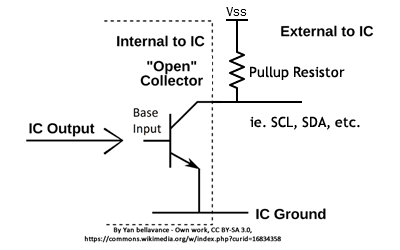
References
Jackson Russett's EEPROM Programmer Shield (Rollover):
Links
 Given that ACES is an acronym for Advanced Computer Engineering School it seems appropriate to introduce students to just that: building their own computer processor from scratch. As Ken Shirriff reminds us, "Before the microprocessor era, minicomputers built their processors from boards of individual chips." It is highly instructive for ACES to physically manipulate and explore this precise architecture prior to their undergrad years that will demand far less of you. Alan Kay's 1982 quote provides further inspiration, “People who are really serious about software should make their own hardware”.
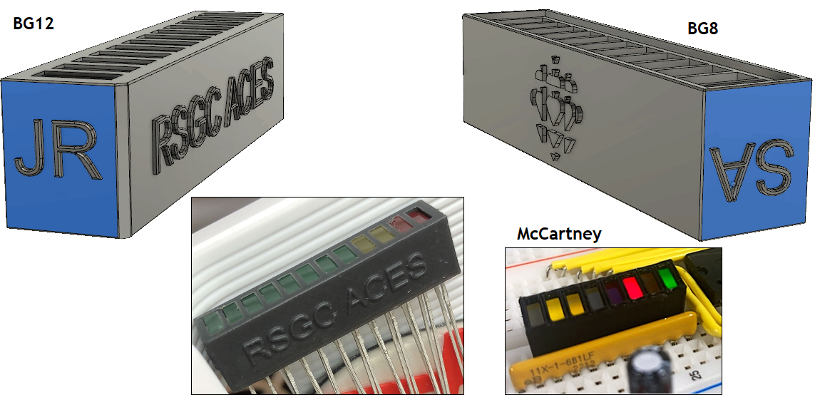