 38.
38. | 2016-2017 TEI4M Assembly Tasks |
AVR TIMERS
38. ![]() Timer1. Fast PWM Mode 15. In this exercise you are asked to develop standalone assembly code that will result in the the horn of your HXT500 standard servo motor sweeping through its 180ˆ of rotation, continuously.
Timer1. Fast PWM Mode 15. In this exercise you are asked to develop standalone assembly code that will result in the the horn of your HXT500 standard servo motor sweeping through its 180ˆ of rotation, continuously.
Task.
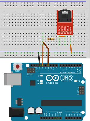
37. ![]() USART Debugging Utility. In this exercise you are asked to develop a utilty that can be used to debug your assembly code by dumping the contents of SRAM the Serial Monitor.
USART Debugging Utility. In this exercise you are asked to develop a utilty that can be used to debug your assembly code by dumping the contents of SRAM the Serial Monitor.
Task.
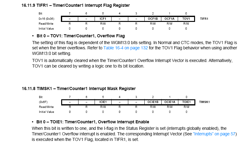
![]() 36.
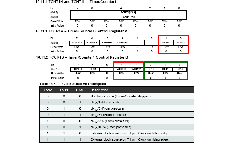
36. ![]() Timer1. Clear Timer on Compare Match. Modes 4 (Output Compare) and 12 (Input Capture) result in the TCNTn clearing (0) when it matches the preset OCRnA/B register. The attached pins can be cleared, set or toggled. This is somewhat easier to use than setting the start count less than the TCNTn resolution an climbing all the way to the overflow. The
OCRnA/B register can be manipulated in the COMPA/B ISR to modify the resulting PWM Signal.
Timer1. Clear Timer on Compare Match. Modes 4 (Output Compare) and 12 (Input Capture) result in the TCNTn clearing (0) when it matches the preset OCRnA/B register. The attached pins can be cleared, set or toggled. This is somewhat easier to use than setting the start count less than the TCNTn resolution an climbing all the way to the overflow. The
OCRnA/B register can be manipulated in the COMPA/B ISR to modify the resulting PWM Signal.
Task.
 decreases.
The mono waveform, recorded in stereo, is shown to the right as it appears in Adobe's SoundBooth.
decreases.
The mono waveform, recorded in stereo, is shown to the right as it appears in Adobe's SoundBooth.
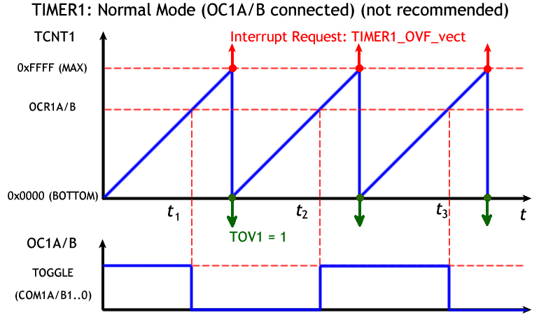
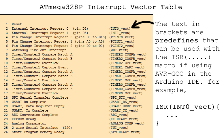
35. ![]() Timer1. Normal Mode with Output Compare (Software and Hardware Interrupts). In addition to a strictly hardware output response to the occurrence of a Compare event, on A and/or B, one can add a software response as well.
Timer1. Normal Mode with Output Compare (Software and Hardware Interrupts). In addition to a strictly hardware output response to the occurrence of a Compare event, on A and/or B, one can add a software response as well.
Task.
	.global TIMER1_COMPA_vect
	TIMER1_COMPA_vect:
 		...
  	reti
 34.
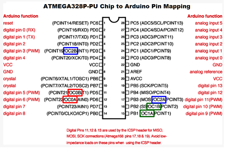
34. ![]() Timer1. Normal Mode with Output Compare (Hardware Intr). A closer look at the pin mapping of the Arduino reveals 6 digital pins with alternate functionality labelled OCnX (pins 3,5,6,9,10,& 11).
Timer1. Normal Mode with Output Compare (Hardware Intr). A closer look at the pin mapping of the Arduino reveals 6 digital pins with alternate functionality labelled OCnX (pins 3,5,6,9,10,& 11).
These pins can be configured to change their state (cleared, set or toggled) when the timer counter register pair (TCNT1H:TCNT1L) matches the value preloaded into the Output Compare Register pair (OCR1A/BH:OCR1A/BL). Note: Since this functionality is achieved strictly at the hardware level (no software ISR required) it is offers maximum efficiency.
Task.
Imagine if we knew about timers back in Grade 11 when we undertook Challenge 1? We could have controlled the PoV with perfect precision.
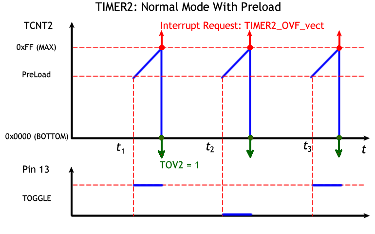 33.
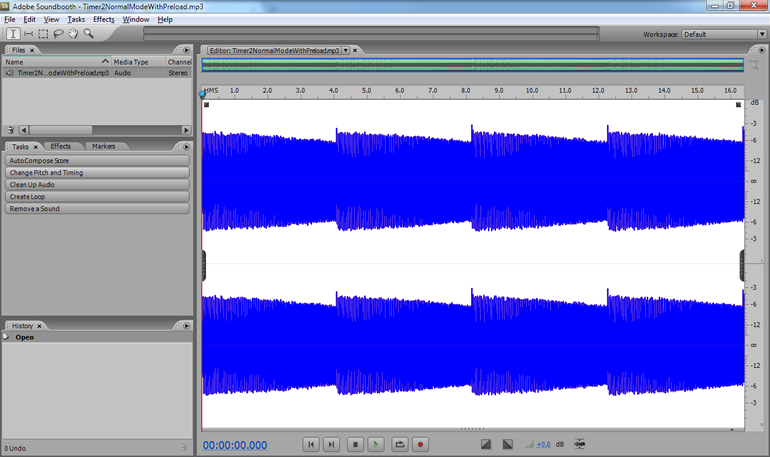
33. ![]() Sound: Timer2 Normal Mode with PreLoad. In the previous exercise you simply let the Timer's counter run freely, restarting at 0x00 on the overflow. In this exercise you are asked to undertake an audio exploration of Timer2's Overflow Interrupt (in Normal Mode) while manipulating the TCNT2 register.
Sound: Timer2 Normal Mode with PreLoad. In the previous exercise you simply let the Timer's counter run freely, restarting at 0x00 on the overflow. In this exercise you are asked to undertake an audio exploration of Timer2's Overflow Interrupt (in Normal Mode) while manipulating the TCNT2 register.
In this exercise you are asked to toggle Pin 13 with Timer2 Interrupt Overflows so as to recreate the provided audio file.
Task.
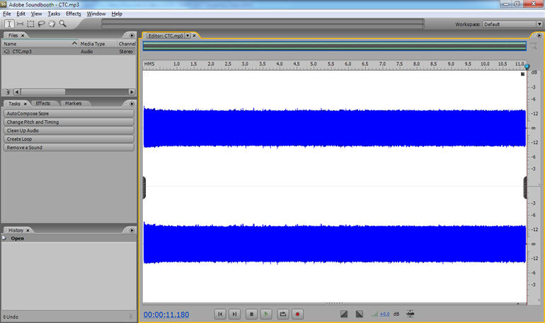
 the volume remains relatively stable while the frequency (pitch) increases. The mono waveform, recorded in stereo, is shown below right as it appear in Adobe's SoundBooth.
 32.
32. ![]() Sound: Normal Mode. Almost a year ago to the day we explored the Arduino's tone() function. Many good high-level theory and practical references exist and here is one of them. It has been determined that the human ear can respond to frequencies in the range from 20Hz to 20KHz. We'll see. In this exercise we're going to undertake a low level exploration of tone generation and listen to the waveforms capable of being generated in Normal Mode from the various timers on the ATmega328P.
Sound: Normal Mode. Almost a year ago to the day we explored the Arduino's tone() function. Many good high-level theory and practical references exist and here is one of them. It has been determined that the human ear can respond to frequencies in the range from 20Hz to 20KHz. We'll see. In this exercise we're going to undertake a low level exploration of tone generation and listen to the waveforms capable of being generated in Normal Mode from the various timers on the ATmega328P.
Task.
  void setup(){
      pinMode(11,OUTPUT);
  }
  void loop() {
     for (int i=0; i<255; i++) {
           analogWrite(11,i);
           delay(30);
     }
  }
You will recall that the parameter to the analogWrite() function affects the duty cycle (Mark/Space ratio). Frequency and volume are the two primary audio charateristics you'll experience. Which of the two are affectd by the changing parameter? Does this make sense?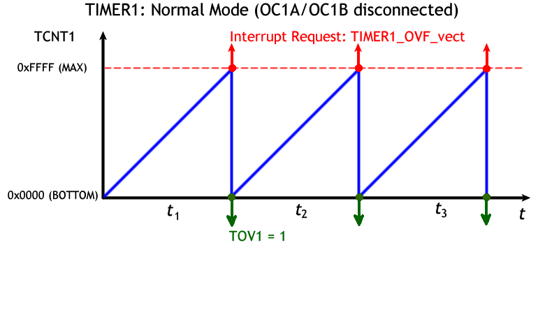 31.
31. ![]() Timer1. Normal Mode. The simplest of Timer1 modes results in the system clock incrementing its 16-bit register pair TCNT1H:TCNT1L with every tick. At 16MHz (`2^24`), the count will reach the top (`2^16`), 256 times per second. The use of one of the prescalers can slow the accumulation down.
Timer1. Normal Mode. The simplest of Timer1 modes results in the system clock incrementing its 16-bit register pair TCNT1H:TCNT1L with every tick. At 16MHz (`2^24`), the count will reach the top (`2^16`), 256 times per second. The use of one of the prescalers can slow the accumulation down.
When the count overflows, an interrupt overflow (TIMER1_OVF_vect) is generated and the count continues from 0x0000 whether you service the request or not. Setting the TOIE1 bit in the TIMSK1 register allows your code to respond to the request. Review the document, Timer1InterruptNormalMode.docx. I have provided both a mid-level implementation of a Timer1 Normal Mode Overflow Interrupt Routine to ease you into the register configurations, followed by the equivalent low-level standalone assembly version in which the ISR toggles an LED on PB5 (digital pin 13 on the Arduino) at rate of 60Hz (120 ovf/s). (Note: although 24Hz is the understood threshold for Persistence of Vision I found this far too low. Even at 40Hz, flicker is detectable. 50-60Hz is more like it)
Task.
 Create an Arduino project entitled Timer1InterruptNormalMode and add the file, Timer1Interrupt1NormalMode.S. Be sure to leave the high-level file Timer1InterruptNormalMode.ino blank. Note: For future reference, you may wish to copy the mid-level version from the document and paste it in as the .ino version, as long as it is completely commented out.
THE STACK (Stack Pointer: SP) ( __SP_H__ : __SP_L__ )
30. ![]() Sum of a Series 2. Recursion is a programming strategy in which a function calls itself to solve a simpler version of the problem until the process reaches a trivial base case. Review the sketch below.
Sum of a Series 2. Recursion is a programming strategy in which a function calls itself to solve a simpler version of the problem until the process reaches a trivial base case. Review the sketch below.
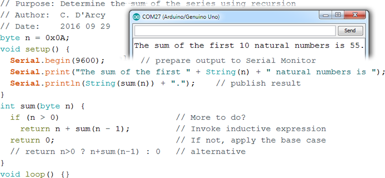
In this exercise you develop an assembly language equivalent as a means to understanding the uses of the STACK to pass values and address between callers and receivers.
![]() Note. On second thought, I don't recommend doing this exercise. Few people in their right mind would attempt this. It took me two days to figure this out. Here's the Excel spreadsheet I used to work out the logic if you're interested.
Note. On second thought, I don't recommend doing this exercise. Few people in their right mind would attempt this. It took me two days to figure this out. Here's the Excel spreadsheet I used to work out the logic if you're interested.
29. Subroutine: Add. The sketch below presents a somewhat formal, high-level solution to adding two bytes with the support of a function (Assembly: Subroutine). What we're interested in, in this exercise, are the details of the passing of the input parameters to the function and the receipt of the return parameter. With this knowledge, you can undertake an assembly language version of this code.
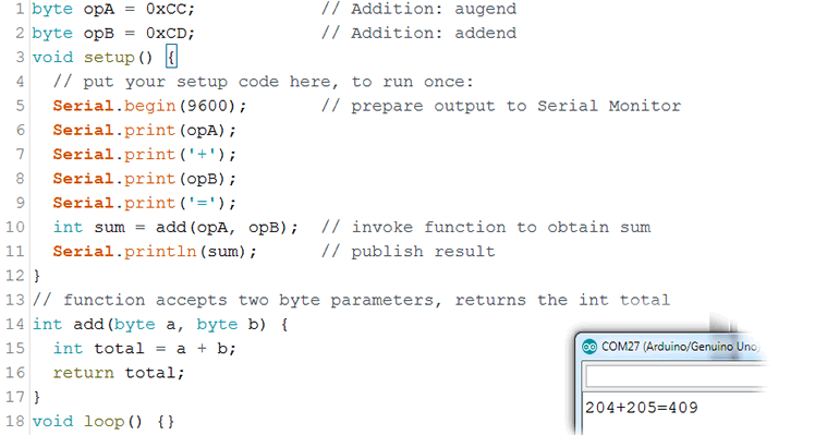
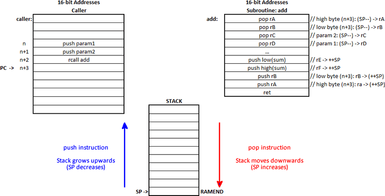
The graphic to the right is intended to show the relationship between the Caller code, the Subroutine and the role played by the Stack in ensuring the communication between the two takes place accurately. I'll be better able to explain how it all works when we're together.
Task. Develop a sketch entitled AddSubroutine.ino that mimics the high-level code above. Incorporate all the best assembly language practices we have highlighted so far.
28. Swapping 3. (push, pop) Declare and initialize two global variables to different values. Implement assembly language instructions to accomplish the same result as Swapping 1 but makes use of the Stack instead.
 26. Matrix Position. For a final look at input polling, develop MatrixAnimation.ino. The assembly code monitors FOUR push buttons for position data before uploading column and row data to two shift registers connected to your 788BS.
The result is that a single LED dot moves about on your matrix as demonstrated in the adjacent animation.
 25. Bargraph Position. Using your Arduino, develop the assembly project BargraphPosition.ino that polls TWO push buttons to control left and right movement of a bar on your bargraph. A single shift register is to be employed to provide the byte data to the bargraph.
 24. Multiple Inputs. In this exercise you are asked to attach three buttons to PORTD pins, one for the red, green, and blue results on an RGB LED. The three buttons are also wired through OR logic (a three-input IC would be great or two cascaded two-input gates) to a single PORTD pin that is polled continuously. Once a state change has been detected, poll the three buttons and light the respective LED for 2s before repeating the exercise.
 23. Input Polling (in,out,sbi,cbi,sbrc,sbrs,sbic,sbis).
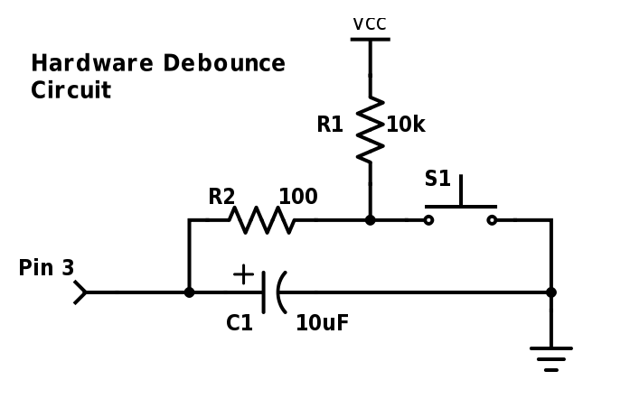
We'll get to interrupts later in the course, but for now you are asked to attach a hardware-debounced button to a port pin of your ATtiny85 and monitor it for a state change. Once recognized, turn an LED on for 3s before repeating the exercise. AVR Delay Loop Calculator.
Note: There are three I/O registers associated with each Port. i.e. DDRB, PORTB, and PINB
23. Input Polling (in,out,sbi,cbi,sbrc,sbrs,sbic,sbis).
We'll get to interrupts later in the course, but for now you are asked to attach a hardware-debounced button to a port pin of your ATtiny85 and monitor it for a state change. Once recognized, turn an LED on for 3s before repeating the exercise. AVR Delay Loop Calculator.
Note: There are three I/O registers associated with each Port. i.e. DDRB, PORTB, and PINB
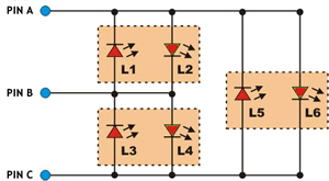 22.
22. ![]() Charlieplexing. The use of shift registers is a hardware solution employed to extend the reach of logic beyond the number of I/O pins on your microcontroller. If the goal is to simply drive more LEDs than the number of microcontroller pins available, a purely software solution is Charlieplexing. The key to successful implementation of this technique is the three-state logic capability of the microcontroller's digital I/O pins meaning the pins can be in one of three states: Output (H)IGH, Output (L)OW and Input (Z) . Placing an I/O pin in the Input (Z) or high impedance state effectively disconnects the pin from the LED network. As can be imagined, given n digital I/O pins, a network of n2-n LEDs can be driven. This is simply the permutation defined by,
Charlieplexing. The use of shift registers is a hardware solution employed to extend the reach of logic beyond the number of I/O pins on your microcontroller. If the goal is to simply drive more LEDs than the number of microcontroller pins available, a purely software solution is Charlieplexing. The key to successful implementation of this technique is the three-state logic capability of the microcontroller's digital I/O pins meaning the pins can be in one of three states: Output (H)IGH, Output (L)OW and Input (Z) . Placing an I/O pin in the Input (Z) or high impedance state effectively disconnects the pin from the LED network. As can be imagined, given n digital I/O pins, a network of n2-n LEDs can be driven. This is simply the permutation defined by,
`P(n,2)=(n!)/((n-2)!)=n(n-1)=n^2-n`
Task.
| PIN A | PIN B | PIN C | |
|---|---|---|---|
| L1 | L | H | Z |
| L2 | H | L | Z |
| L3 | Z | L | H |
| L4 | Z | H | L |
| L5 | L | Z | H |
| L6 | H | Z | L |
Research Links.
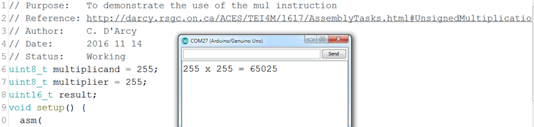
21. Multiplication (mul, muls, mulsu).The AVR Instruction Set breaks down the multiplication of 8-bit operands into three cases: mul (unsigned×unsigned), muls (signed×signed), and mulsu (signed×unsigned). Regardless of which registers contain the operands, the 16-bit product is always placed in the r1:r0 register pair. You are asked to develop an example of each.
Note 1. The avr-gcc compiler supports numerous integer types. Use the correct one in each context below.
Note 2. It appears that the Serial library uses r0 and r1 for its own purposes and prevents the assembly code from obtaining correct results. Delay the use of the library until after the results have been obtained.
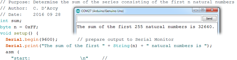
20. Sum of a Series 1. The sum of the first n natural numbers can be expressed as,
`sum_(i=1)^n i=(n(n+1))/2`
Create a sketch entitled SumSeries.ino that begins in a manner similar to the capture below and uses assembly instructions to accumulate the sum. The value of n can be limited to a byte (uint8_t) but the sum must accommodate a uint16_t total. The output appears in the inset.
19. Addition of uint16_ts. (add, adc, eor). Create a sketch entitled AddInts. Declare and initialize two global variables, opA and opB, of type uint16_t and a global variable sum of type uint32_t. Implement assembly language instructions to add the two operands and store the result in sum. Add Serial functions to confirm the result.
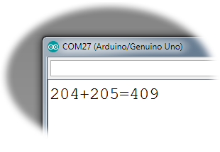
18. Addition of uint8_ts. (add, adc). Create a sketch entitled AddBytes. Declare and initialize two global variables, opA and opB, of type uint8_t and a global variable sum of type uint16_t. Implement assembly language instructions to add the two operands and store the result in sum. Add Serial functions to confirm the result as in,
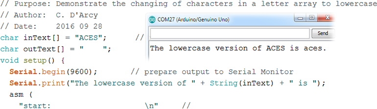
17. ToLowercase 2: char[]. This exercise extends the previous one by asking you to convert all the letters in a char array to their lowercase equivalent.
Develop the sketch, ToLowerCaseCharArray.ino that begins as shown below and yields the output in the inset.
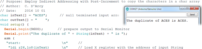
16. ![]() ArrayCopy : char[]. (ld, st, lo8(), hi8()) In this exercise you will employ Indirect Addressing with Post-Increment to duplicate the characters in an input array.
ArrayCopy : char[]. (ld, st, lo8(), hi8()) In this exercise you will employ Indirect Addressing with Post-Increment to duplicate the characters in an input array.
Task.
LOGICAL
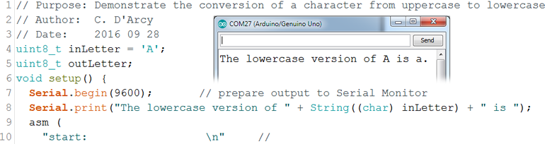
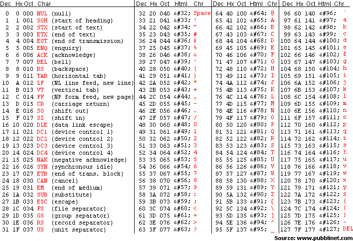
15. ToLowerCase 1: char. You are likely aware that the ASCII Table defines the numeric value of the lowercase letters to be 32 more than their uppercase equivalents. Develop the sketch ToLowercaseChar.ino that employs assembly language instructions to obtain the value of a global variable of type char that defines an uppercase letter and through an appropriate mask, uses a logic instruction to convert it to its lowercase equivalent. Display the result to confirm.
14. OR Mask (or,ori). To ensure specific bits of a register are set while preserving the state of other bits, the or or ori instruction can be employed with the use of a mask. Consider the byte mask 0x0F. Applying this mask to a register with the ori instruction, will result in bits 0 through 3 being set while bits 4 through 7 remain unaffected. Develop the sketch ORIMask.ino that employs assembly language instructions to set the even-numbered bits, while leaving the odd-numbered bits unaffected. You will accomplish this though the design of an appropriate mask applied with the ori instruction. Display the results to confirm.
13. AND Mask (and,andi). Individual bits of a register can be set or cleared through the use of a 'mask' applied with the and instruction. Consider the byte mask 0x01. Applying this mask to a register with the and instruction, will clear bits 1 through 7 and preserve the value of bit 0 in the register. Develop the sketch ANDMask.ino that employs assembly language instructions to clear the upper nibble of a byte, preserving the original contents of the lower nibble. You will accomplish this through the design of an appropriate mask applied with the andi instruction. Display the results to confirm.
FOUNDATIONS
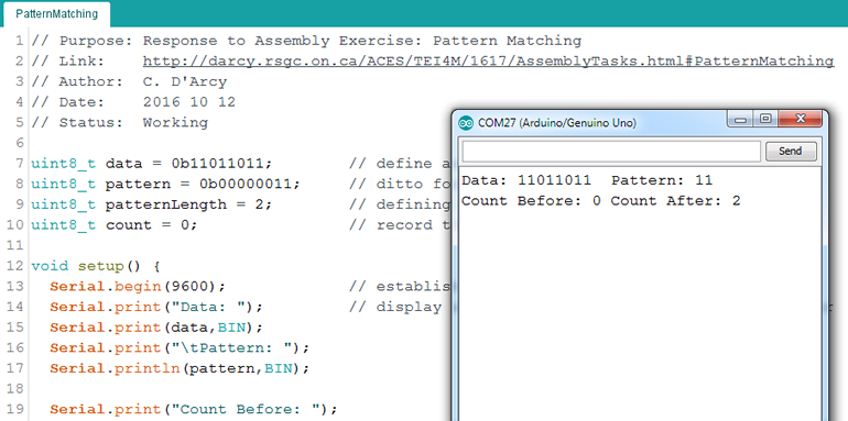
12. Pattern Matching (and, cp, lsr, mov). Searching for a particular sequence of bits within a longer bit sequence is common task. In this exercise you are asked to count the number of occurrences of a bit pattern within a data byte. In the graphic below the number of occurrences of the bit pattern 11 within the byte 11011011 is determined to be 2. One might think it is 3 but, for this exercise, the search starts at bit 0 and advances through the target byte by an amount equal to the number of bits in the sought after pattern.
Task. Create a sketch entitled PatternMatching.ino, and start it off as shown below. Complete the assembly statements that lead to the results as shown in the inset.
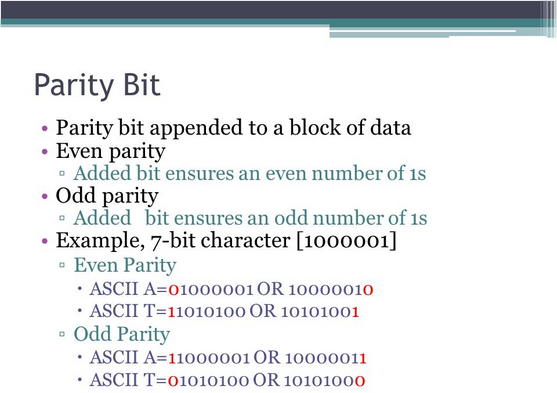
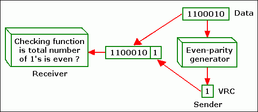 11. Parity. In the early days of computing, communication between computers was particularly vulnerable to noise (static) on the lines resulting in errors (dropped bits) in transmission. A strategy developed to reduce the number of errors was for the transmitting and receiving devices to first agree on whether bytes transferred would ALWAYS contain an EVEN or ODD number of bits. A dropped bit could be detected if the number of bits received did not reflect the agreed-upon protocol. Since the basic ASCII table only required 7 bits of information, the eighth bit (sometimes referred to as the parity bit) would be SET or CLEARED depending on the protocol.
 Task.
Task.

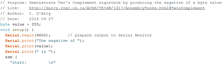
10. Two's Complement. In deciding on a strategy for storing negative numbers (given there's no minus sign), computer scientists decided the highest priority was to ensure a number and it's negative added up to 0. The strategy they came up with for determining the negative of a number, that all computers today have adopted, is known as the Two's Complement algorithm. Look up the neg instruction and it declares it to be Two's Complement right in the title!
Tasks (4).
1. Research the Two's Complement algorithm. What is the One's Complement? Apply the Two's Complement to a binary byte value using pencil and paper. What would result if you applied it twice? Try it.
2. Develop the sketch NegativeByte.ino that uses the neg assembly instruction to produce the negative of a global byte variable. Display to confirm. Observations?
3. Develop the sketch, TwosComplement.ino, along the lines of the code below that uses the assembly language instructions to determine the negative of the value variable without using the neg instruction. Display the result to confirm.
4. The neg instruction only operates on a single register (8-bit). Develop the sketch NegativeInt.ino that employs assembly language instructions to determine the negative of a global uint16_t (exactly 16 bits). Display the results to confirm with the BIN modifier.
9. Swapping 2. Declare and initialize a global variable of type uint8_t to 0xF0. Implement assembly language code to interchange the high and low nibbles before assigning the new value back into the global variable. Display the results to confirm.
8. Swapping 1. Declare and initialize two global variables to different values. Implement assembly language instructions to first, load the value into registers, and then interchange the values of the registers, then store the new values back into the global variables. Display the results to confirm.
7. Bit-Shifting (lsl, lsr, rol, ror, asr, lsr). Examine, and be able to explain the difference between of each of these six bit-shifting functions. Identify which ones can be considered 'destructive' in that the contents of the register they operate on is permanently altered?
6. Branching. The Program Counter, PC, is a two-byte register that always holds the address of the next instruction to be executed. Normally, after an instruction has been fetched from Program Flash' and placed into the Instruction Decoder, the Program Counter is incremented by 1, as in PC←PC+1. However, there are 20 branch instructions that cause the Program Counter to increase by a value other than 1, as in PC←PC+k. Each of the four-letter mnemonics for these instruction begin with the letters BR. Look them over and try to remember their unique purpose.
5. Load, Test and Increment a Global Variable (lds, tst, inc, sts). Declare and initialize a global variable of type byte. Load the contents of the variable directly from SRAM (lds) and test (tst) whether the value is zero, lighting LED 13 if it is. In any event, add one to the variable before storing the value back in SRAM. Use Serial.println statement to confirm the increment took place.
4. Streamlining. Rewrite a more more streamlined version of the previous BlinkwithDelay code that uses on a single asm() statement in each of the setup() and loop() functions.
 3. Bargraph Flasher (ser, out, com). You're aware that sbi and cbi are convenient for setting and clearing individual bits in an I/O register. The ser instruction sets ALL bits in a GP register. Alternatively, to set multiple bits in an I/O register, the out instruction is used. All bits in a register can be inverted through the use of the com instruction.
Task.
1. Wire the rightmost 8 LEDs of your bargraph to the PORTD pins on your Arduino.
2. Develop assembly language instructions within a sketch called BargraphFlasher.ino that results in the effect displayed in the adjacent animation.
2. Blink with Delay (ldi, rcall, dec, brne, rjmp). In this code the Arduino C delay(ms) function is replaced with an assembly function that does the same thing (waste clock cycles).
1. Blink (sbi, cbi). In the Example Blink sketch, replace the pinMode(13,OUT); , digitalWrite(13,HIGH); , and digitalWrite(13,LOW); statements with their Assembly equivalents.