 There are no quizzes, tests, or exams in our ACES program. Put another way, you are NEVER put into the position of having a dramatically limited amount of time to demonstrate the skills you have acquired. You can invest as much (or as little) time into your reports as you choose. In return for being granted complete control over the depth and quality of your submissions I can place a premium on detail, precision, and the pursuit of perfection. So, my advice to you if you want to become exceptional is to follow the written and oral instructions carefully and, beyond the required elements of each report, demonstrate tasteful and appropriate creativity and imagination to distinguish yourself from the mediocre. Good luck and, remember, the race is long but it's over quickly.
Reports. Required Elements
If you do not submit your report by the deadline specified, you receive a mark of 0. This is done as a favour to you to help you appreciate that the real world will dismiss you if you can not demonstrate responsibility and accountability. You are to archive ALL of your reports in the single Word document, DER.docx. The first page is your Title page, followed by a multi-page Table of Contents, after which your reports begin. EACH report will start at the top of the next new page and, unless otherwise specified, consist of the following sections, in the order listed,
Purpose
Reference
Procedure
Media
Reflection
The vast majority of us can tell the difference between quality and rubbish in an instant. As a young scholar you have to decide what your name will stand for. It should matter very little whether you enjoy a task or not; if you're going to attach your name to something it is a direct reflection of who you are.
Project 1.3. The Counting Circuit
 This final activity provides a simple introduction to fundamental capabilities of many digital devices: counting and display. There are a number of stages or subcircuits in this system and your DER will clearly present the role played by each.
Start your DER with a big picture Theory section,
written in your own words that mentions, generally, the input to the system, the generation of a clock signal consisting of pulses having both a duration and a frequency, culminating in the presentation of the pulse count on the display device. This would an ideal place to present a detailed, margin-to-margin Fritzing diagram, breadboard or (organized) schematic view, to introduce your readers to the full prototype you are about to describe and discuss in three pages that follow.
A Note on Graphics. Graphics should support the text they are illuminating. Poorly composed photos, sloppy and inconsistent choices for diagrams like pinouts and schematics work against you as they can confuse your readers and leave them with a sense that the author doesn't care about his presentation so why should they?
Follow the Theory Section with the eight subsections (A-H) described below. For the first section, Analog Input, include, as a graphic, that part of the schematic that it pertains to. The next five sections (B-F) subsections should include a Reference Section that includes the respective live hyperlink appearing below:
Following the Reference Subsection within each of the five areas, include a Purpose section (this one could go before the Reference Section)
describing in detail, how each stage contributes to the sequence. Be sure to clearly present the input, processing, and output of each stage, supported by informative, attractive, and well-formatted graphics.
Following the final subsections include Media (captioned photos and video) and Reflection sections.
A. Button Input
- Purpose (discuss the momentary PBNO and its pullup resistor configuration)
- Include your own breadboard/schematic diagram, right-aligned, to
support your discussion.
B. NAND Gate Oscillator (4011)
- Procedure
- Explain, in detail, the function of this chip (Input, Processor, Output)
- Explain the concept of analog input to digital output and how this
chip accomplished this
- Include
a discussion of the pin diagram in this
IC
- Explain what a clock signal is
- Discuss the role played by RC1 and RC2 and the role played by its respective capacitors and resistors.
- Pinout diagram taken from the web and your own breadboard /schematic of the wiring and supportive analog components
C. Decade Counter (4017)
- Procedure
- Explain, in detail, the function of this chip (Input, Processor, Output)
- Explain what it means to ensure ALL of the input pins must be conditioned and
how this is done
- Explain why Pin 12 is referred to as the Divide-by-10 pin with respect to the input and output clock signals.
- Pinout diagram taken from the web and your own breadboard /schematic of the wiring.
D. Decimal Counting Binary Up/Down Counter (4510)
- Procedure
- Explain, in detail, the function of this chip (Input, Processor, Output)
- Create a two-column table with rows for all 16 4-bit binary values in the
left column and their equivalent decimal values in the right column
- Pinout diagram taken from the web
E. Binary Counting Decimal Decoder (4511)
- Procedure
- Explain, in detail, the function of this chip (Input, Processor, Output)
- Explain the purpose of the Blank, Store, and LampTest pins and how they must
be conditioned for normal use.
- Pinout diagram taken from the web
F. Seven-Segment Display
- Procedure
- Explain, in detail, the function of this component
- Explain the difference between the Common Anode (CA) and Common Cathode (CC)
versions of this component. Which one did we use?
- Explain how the pins on the 4511 and 7-seven segment make the wiring straightforward.
- Explain why each pin on the display requires its own resistor.
- Graphic (google a similar small image)
- Pinout diagram taken from the web
G. A Counting Circuit PCB
Update: See email post on Thursday December 17 to the ICS2O Conference regarding Stages G and H.
Soldering Advice and Tips for (Qualifying( Fall 2020 ICS2O-E ACES.
- The Hare lost. The Tortoise, on the other hand, read ALL the tips below before even thinking about beginning. He won.
- Watch N. Vassos' ACES' Soldering Video for some great tips. Watch is again even if you have seen it previously.
- DO NOT BE HASTY. Take your time with this and double-check with the Forum if you are not sure to avoid disappointment and a reduced mark for the careless.
- The supplementary parts shown in the photo below wil be mailed to qualified ACES on Monday December 21.
- In addition to these parts, you will need to supply 2-10 KΩ, 2-1 MΩ and 1 470 Ω fixed resistors from your inventory.
- In place of the 10 μF electrolytic capacitor, I have provided a compact 100 μF capacitor for longer duration.
- Your soldering pen should be no hotter that 300°C, and you should take no more than 3s per solder joint to avoid compromising your component.
- Solder the smaller components first, working upwards to the larger ones.
- The IC Sockets (chip seats) have a notch in them. Orient them to match the silk screen notch. DO NOT SOLDER THE SOCKETS WITH THE IC IN THE SEAT. ICs are placed in the seat after soldering to avoid any exposure to heat.
- AFTER the IC Sockets are soldered, you can place your ICs in them (4011, 4017, 4510, 4511), ensuring the reference notches match the silk screening of the PCB (and, hopefully your sockets)
- Line up the resistor network so the dot matches the silk screen indication (left).
- Solder the 7-Segment Display in LAST. By this time you will be more relaxed and more confident. Remember, 3s per joint, max.
- Do not solder a power connector to the PCB as I'll provide a superior one with the case if this stage is successful.
- For the novice solderer (you), solder regularly runs into close, adjacent empty holes. Without the right equipment it can be almost impossible to remove it. For this reason, I strongly urge you to consider placing the secondary in its hole so that if the solder runs, no problem, the part is already there!
- Finally, of the extra parts I have supplied only three of them did not come in your original kits (the PCB and the two resistor networks). I have chosen to give you replacements partly for esthetics, partly for performance (pricier kinked IC Sockets) and possibly because for possible loss or failure of the originals.
Once the prototype media has been obtained for your DER (photos and video), ACES wishing to extend their engineering skills are encouraged to convert their breadboard prototype to a more permanent device. A custom printed circuit board was designed and manufactured expressly for the use by Jr. ACES for this purpose. Interested ACES should present their working prototype to Mr. D'Arcy at least TWO days prior to the DER due date in order to receive their PCB. Receipt of such a board comes with the expectation that components will be soldered, the circuit tested, and summarized in text, photos, and video as part of the DER summary for this Counting Circuit project.

H. A Counting Circuit PCB Case
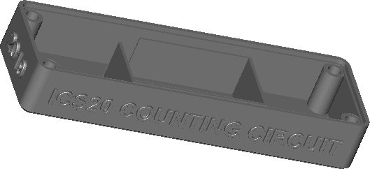 Congratulations on reaching the final stage (8) of our marathon Counting Circuit project! Students that have successfully soldered their PCBs that demonstrate forward (and backwards) counting on the seven-segment display are invited to present their circuit to Mr. D. to receive a custom case designed and printed in the DES by J. Dolgin (ACES '20) into which their device can be mounted. A similar two-colour case was printed on the Ultimaker 3 in 2018 by K. Fiset-Algarvio (ACES '19). Click the image below to view a short time-lapse video of the case being printed,

Power for the device is sourced from a 9V battery inside a compartment within the interior of the case. The leads of a battery snap can be soldered to the correct pads in lieu of an external DC Jack. Be sure to place electrical tape across the battery to insulate it from the bottom of your PCB to prevent the possibility of shorting. Finally, screw the assembly together and fully test, prior to capturing the final frames of your project video.
Finally, be sure to address ALL issues from previous submissions and update your Table of Contents before attaching DER.docx to an email to handin under the Subject Line: A Counting Circuit (Complete)
Project 1.2. The Full Adder or The Two-Bit Adder (pick one)
Students can elect to complete either the Basic or Advanced task described below. Some of you have struggled with the challenges of this course but this Basic task is quite doable if you are organized, start early, and take advantage of the wide support offered you.
Those of you intending to continue on into our Grade 11 course should consider completing the Advanced assignment for the extended prototyping practice and deeper conceptual understanding.
 The Full Adder (Basic)
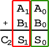
Our recently-completed session introduced you to the digital logic gates. These are the computer's primary operators in much the same way as addition and multiplication are the primary mathematical operators. One of many useful circuits involving logic gates is the circuit that allows computers to perform addition of binary (base 2) numbers.
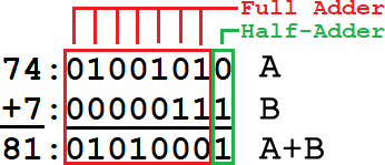 The graphic to the right is meant to reveal how the computer 'sees' the addition of 74 and 7, packaged as 8-bit numbers. Similar to humans, the computer proceeds from right-to-left, adding pairs of binary numbers (0 and 1). For the first addition (green) there is no 'carry in' number from a previous addition. This requires a circuit known as a half-adder. For each of the remaining seven additions (red), the computer must add the two binary operands (A and B) but must also add in the binary number carried from the previous addition (C). A circuit that performs this is referred to as a full-adder.
Although many of you likely could, Grade 10 students are not expected to have come up with the circuit designs for the half and full adder circuits, but a good grasp of why the work and the correct outcomes they produce provide deep mental satisfaction. To this end you are encouraged to spend time interacting with the relevant combinational example provided as Falstad simulations,
- Half-Adder: https://tinyurl.com/yehzn8gc
- Full-Adder: https://tinyurl.com/ydomt5mp
Task.
- Jr. ACES are required to develop the breadboard prototype for the full adder circuit. This requires three input buttons (A, B, and C) and two output LEDs indicating the Sum and Carry bits, as well as the 'Processor' consisting of the wired-up logic gates.
- Again, using the DER returned to you, and taking into account the personal and general feedback comments you have been provided with, start this report on first new page, after the The Analog Oscillator Report. Add the Project name in Heading 1 Style and complete sections under the subheadings: Purpose, Reference, Procedure, Media, and Reflection. Text is developed in accordance with the recommendations for Technical Writing and reflective of your much-improved formatting abilities. Graphic manipulation is undertaken according to the specifications laid out in the Engineering Report General Guidelines.
- Students should note that since the layout for this circuit was provided to you in class: https://mail.rsgc.on.ca/~cdarcy/darcy/ACES/TEL3M/IPEVO/FullAdder.fw.png the mark you receive for this submission will be based on the clarity of your circuit presentations and quality of your DER based on your response to the expectations, feedback, and support provided you.
- Attach your DER to an email to handin with the Subject: The Full Adder by Saturday May 1 at midnight.
 The Two-Bit Adder (Advanced)
Task.
 After sufficiently researching the half- and full-adder circuits, you are to wire up a prototype on a breadboard that demonstrates a two-bit adder. This would demonstrate the limited sum of two operands, each from 0 to 3, for a sum over the range from 0 to 6.
- Parts will include 4 push buttons (or slide switches) for inputs A and B inputs, three LEDs for outputs, and the required CMOS ICs as the processor that integrates both a half and full adder.
- There are many ways to demonstrate both your knowledge and your passion for this material. Utilities such as Fritzing, TinkerCAD Circuits, Falstad, etc. all offer ways to enhance you reader's experience. You do not need to include all of them as creating a strong report is NOT about checking all the boxes possible. Pick one or two you are drawn to and exploit their capabilities to teach the reader about how digital logic gates can be combined to perform the addition of a pair of two-bit binary operands.
- Attach your DER to an email to handin with the Subject: The Two-Bit Adder by Saturday May 1 at midnight.
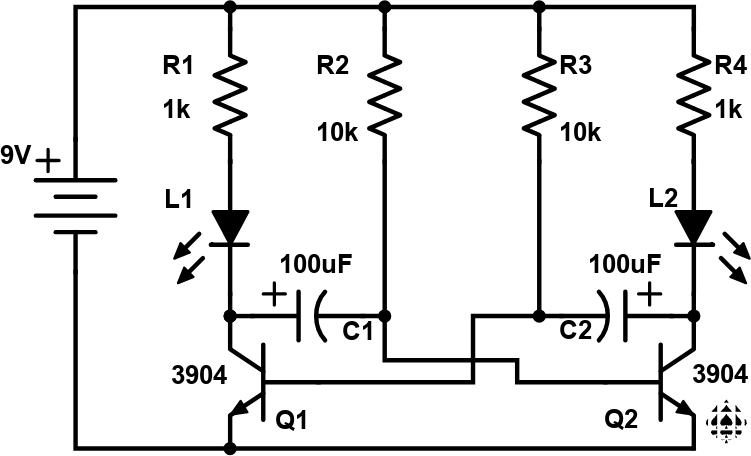
Project 1.1. The Analog Oscillator
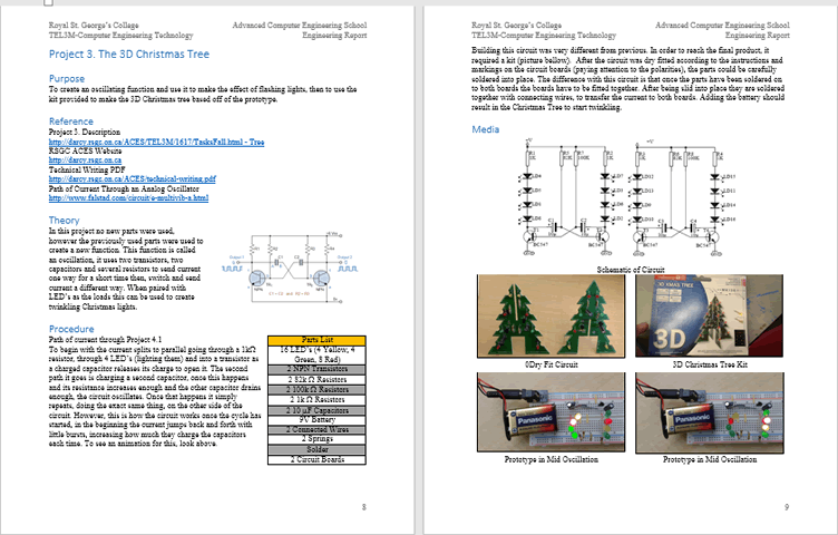
The Square Wave, a highly orchestrated sequence of alternating high and low durations, is the backbone of modern, digital, communication. The purpose of this project is to introduce you to the transistor and to demonstrate how it can be combined with other familiar analog components to produce an oscillating signal with properties similar to the digital square wave.
Task.
- Clean the lens of your phone's camera, as you will be gathering media (photos and videos) throughout this project, from start to finish, in support of your DER project summary due Saturday March 27.
- This project will test your organizational abilities as much as your nascent electronics' knowledge and skills. Part of the task includes thinking deeply about what you're doing.
- After studying the schematic of the Analog Oscillator below left undertake your prototype (aka, blinker, Astable Multivibrator) on your breadboard. When you are confident the circuit has a chance of functioning, apply 9V power. Debug as necessary and document the results with your phone's camera.
You may wish to experiment with the rate at which the LEDs are flashing by adjusting the sizes of the resistors and capacitors.
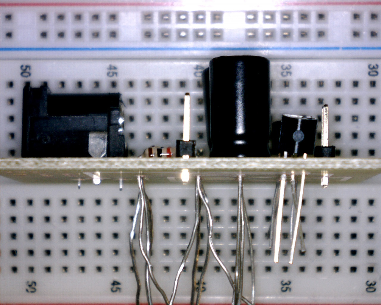
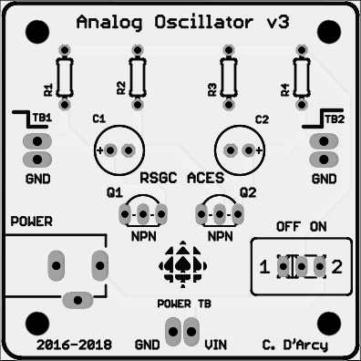
| The Analog Oscillator Schematic |
PCB: Dry Fit |
 |
 |
- DER. Starting on the first page after the Table of Contents, add the Project name and complete sections under the subheading: Purpose, Reference, Procedure, Media, and Reflection. Text is developed in accordance with the recommendations for Technical Writing and reflective of your formatting abilities. Graphic manipulation is undertaken according to the specifications laid out in the Engineering Report General Guidelines.
- Attach your DER to an email to handin with the Subject: The Analog Oscillator no later than Saturday March 27.