 Analog to Digital Conversion
| M. Yamada's SAR ADC (Last Update: 2026 01 19 |
Analog to Digital Conversion
A large sector of the modern digital world is dedicated to interfacing with natural world analog data. Sensors (transducers) are devices that can measure natural phenomena such as sound, heat, pressure, distance, acceleration, flow, force, gas, smoke, methane, etc. and output continuous voltage levels. Microcontrollers possess the functionality to digitize (binary number) these voltage levels through the use of analog to digital conversion (ADC) circuitry.
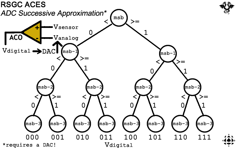
Of the variety of different algorithms and processes ADCs engage, successive approximation is one of the most common.
ADC0804
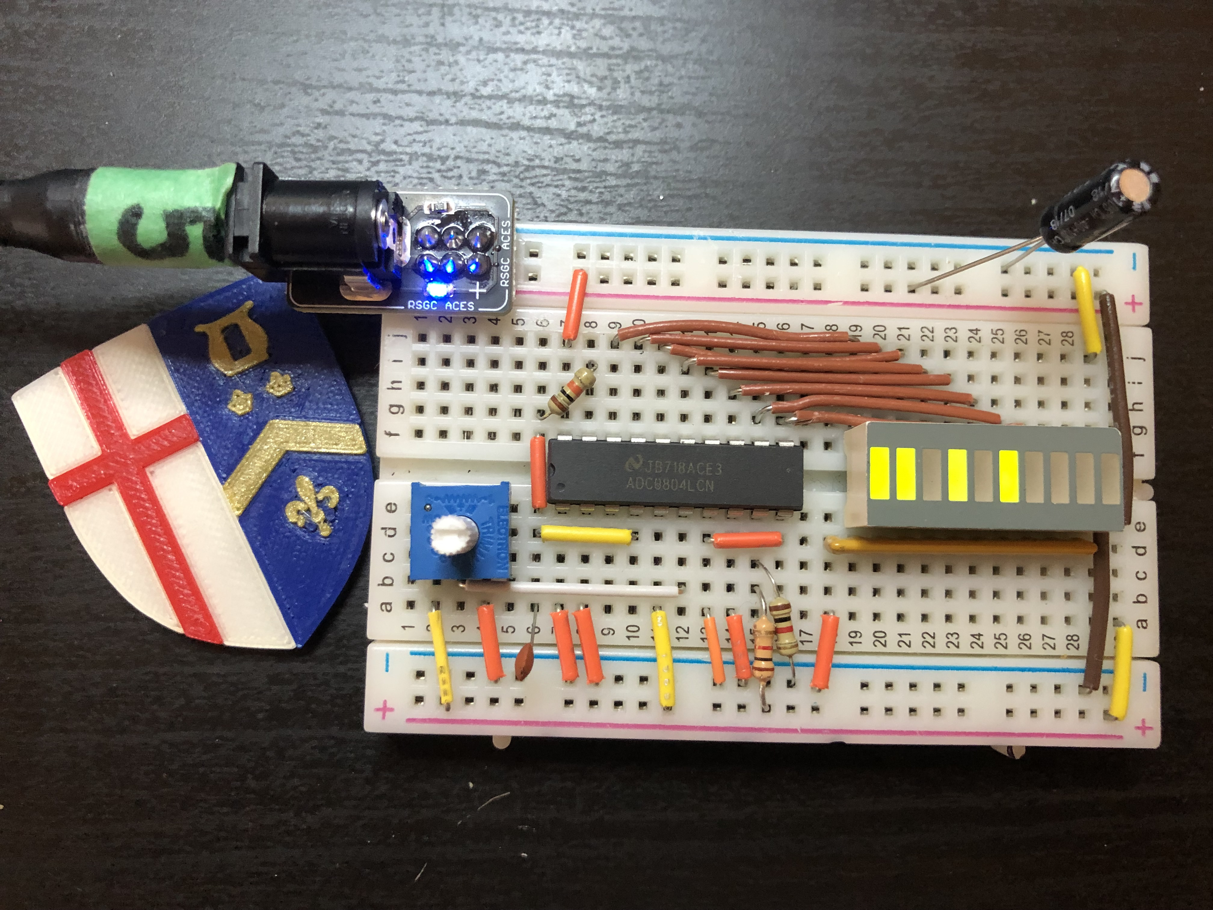 Before the emergence of microcontrollers (μC) with built in ADC functionality, there were microprocessors (μP) that relied on external ICs dedicated to perform the ADC function. One such IC that employed the successive approximation algorithm was the ADC0804. This IC is no longer manufactured.
The photo to the right shows our implementation of the ADC0804 (click to enlarge). As the potentiometer is turned, the LEDs reflect the 8-bit digital approximation to the voltage level (0-5V → 0-255).
Although the ADC0804 is considered obsolete, successive approximation remains a fascinating concept and circuit to prototype.
Hackaday Project
 G. Davidge (ACES '24) pointed us to an intriguing ADC project that he discovered on the Hackaday web site: https://hackaday.io/project/181826-homemade-successive-approximation-register-adc
The ingenious circuit from Mitsuru Yamada undertakes the Successive Approximation algorithm to convert an analog voltage level between 0 and 5V into a 7-bit binary representation.
Implementations
So intrigued were ACES with this circuit that J. Strain (ACES '23) elected to take on the project for his ![]() final Grade 12 ISP.
He made significant headway.
final Grade 12 ISP.
He made significant headway.
J. Rogan (ACES '23) also accepted the project challenge once his final exams were over in early June '23.
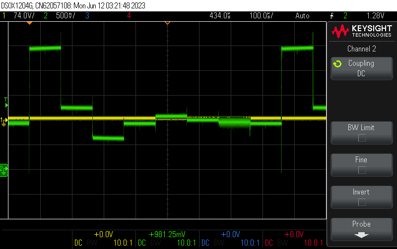
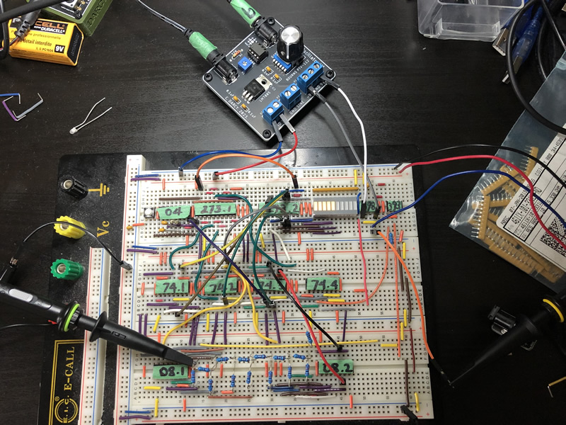
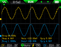
Inspired by what these students were pursuing, Mr. D. took the project on in June '23 with some guidance from the students' experiences. This led to a successful result as shown on the scope image below, left. The prototype appears below, right, albeit with some less-than-impressive wiring.
 |
 |
|---|
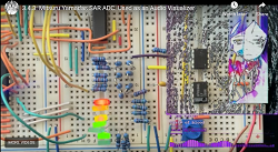
L. McCartney and G. Davidge successfully completed their versions of Yamada's project in March 2024 with these compelling images as evidence.
 |
 |
|---|
E. Hooper and J. Darou-Santos successfully completed their versions of Yamada's project in March 2026 with these compelling images as evidence.
 |
 |
|---|
Bonus
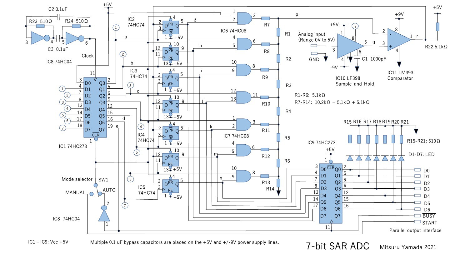
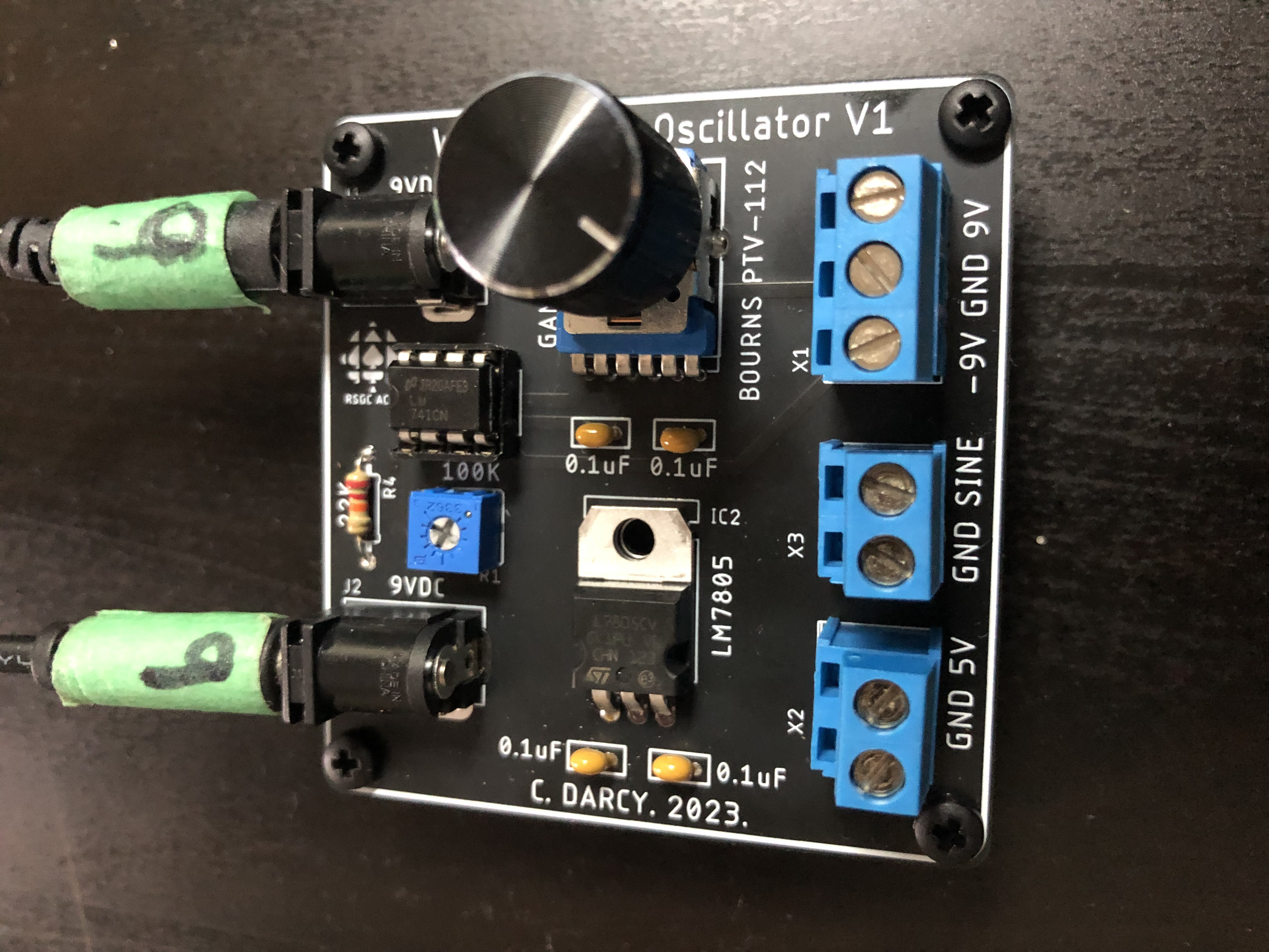 The majority of the ICs in this project are in the 74HC family that require a 5V supply. Two exceptions are the LF398 sample and hold IC and the LM393 op amp comparator that benefit from access to +/-9V supply. To achieve this, a custom power supply was imagined and developed that includes a feature ACES might find useful in this and future projects. The onboard
 ![]() Wien Bridge Oscillator employs an LM741 op amp to produce a sinusoidal wave with a frequency in the 1400 Hz range. A summary of this project undertake in early June '23 can be found at, http://darcy.rsgc.on.ca/ACES/TEI4M/WeinBridgeOscillator/index.html
Wien Bridge Oscillator employs an LM741 op amp to produce a sinusoidal wave with a frequency in the 1400 Hz range. A summary of this project undertake in early June '23 can be found at, http://darcy.rsgc.on.ca/ACES/TEI4M/WeinBridgeOscillator/index.html
Related Concepts
R2R DAC
ADC
LF398 (Sample and Hold)
1. Overview. I can't tell you how many times I've read in ACES Reflections that the author wished he had invested a lot more time at a project's outset understanding the big picture before he started protoyping. Well, this is your chance. You are to begin your report with a general overview of what this device is designed to do and provide specific details on how it accomplishes the task. You can draw on your Grade 10 and 11 experience with analog versus digital concepts, your familiarity with the Arduino's ADC functionality combined with the abundant resources I've provided and your own deep research.
In addition to a multi-access power supply (±9V, 5V and 0V) and a slide switch (Manual vs Free-Running Conversions) your prototype will need the following,
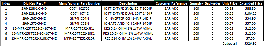
| (Minimum) Yamada SAR ADC Parts | |||||||||||||||||||||||||||||||||||||||||||||||||
|---|---|---|---|---|---|---|---|---|---|---|---|---|---|---|---|---|---|---|---|---|---|---|---|---|---|---|---|---|---|---|---|---|---|---|---|---|---|---|---|---|---|---|---|---|---|---|---|---|---|
|
|
||||||||||||||||||||||||||||||||||||||||||||||||
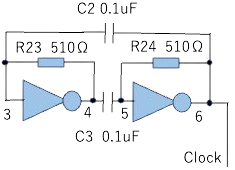 Clock. In addition, we can start this project in a manner similar to CHUMP in that you are asked to prototype the SAR ADC's clock oscillator. Yamada's inverter-based oscillator is intriguiing and worthy of closer examination. Yamada claims that his astable multivibrator design yields a period of 103 μs, suggesting a clock frequency in the order of 10 kHz. Determining the theory behind this claim and confirming it either with a DMM set to Frequency, Falstad (Inverter Oscillator) , CircuitLab, your Nano using interrupts and/or an oscillioscope that will set the stage for its further engagement and graphic output later in the project.
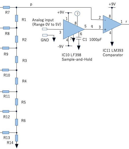
2. Analog Input (Sample & Hold, Comparator, R/2R Ladder DAC). It would be highly informative to construct the analog input to your ADC (assembled from the sample&hold, comparator and 7-bit R/2R Ladder DAC constructed from your 1% 5 kΩ and 10 kΩ fixed resistors).
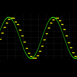
SAR ADC Timing Diagram
Below is the timing diagram from M. Yamada for the operation of his SARADC project,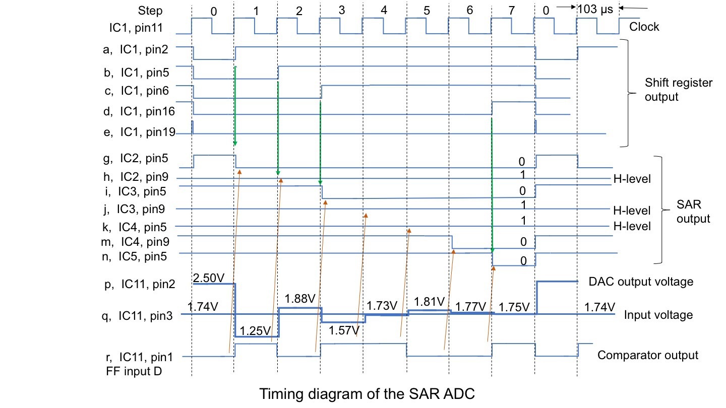
3. Completed. Complete the wiring of your version of Yamada's ADC. Using a potentiometer or some other full-range variable voltage input confirm your version is functional by displaying the 7-bit output on a bargraph or alternative breadboard device.
DMM and/or Oscilloscope monitoring/analysis will enhance your presentation.
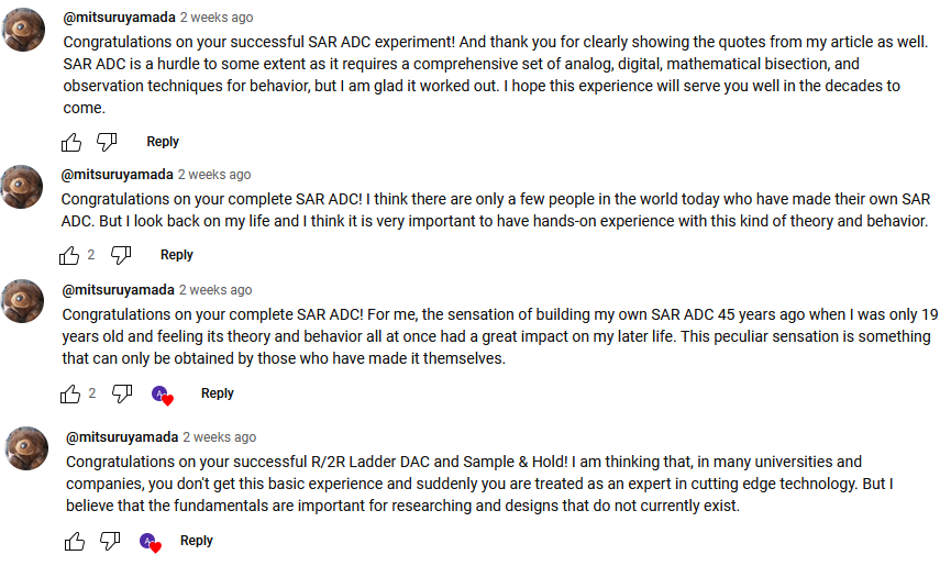
Postscript. After the first successful completion of Dr. Yamada's SAR ADC project by the 2024/2025 ICS4U-E Grade 12 class, Dr. Yamada was contacted and offered the opportunity to view the student videos. Ever the teacher and mentor, Dr. Yamada generously provided feedback, recommendations and encouragement both in emails and comments on each of the videos as shown below.
"On the shoulders of giants..." as they say.