Introductory Exercises (2020 01 22) (Reference: https://en.cppreference.com/w/cpp/language/operator_precedence)
- Create an Arduino sketch for the UNO (328P) entitled BitBanging (You could do this for other AVRs but we could use the services of the Serial Monitor to confirm our results)
- Declare the following variable: uint8_t value = 0; and use it exclusively for the manipulations below. Echo value to the Serial Monitor after each modification.
- With full knowledge of C++'s order of operator precedence to avoid unnecessary brackets, undertake the following, in sequence, within your setup() function,
- set bit 5
- set bit 3, while leaving all other bits unaffected
- clear bit 5, while leaving all other bits unaffected
- invert all bits
- invert only bit 3
- assign value the BCD equivalent of 27
- clear (mask off) the high nibble
- make the high nibble the same as the low nibble
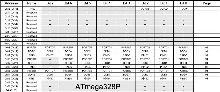
GPIO Register-Level Exercises (2020 01 28) (p. 12: https://mail.rsgc.on.ca/~cdarcy/Datasheets/ATmega328PSummary.pdf)
- How many GPIO Ports does the 328P have? What are their (letter) names?
- How many Registers are associated with each of the ports? What are their names and what are their purposes?
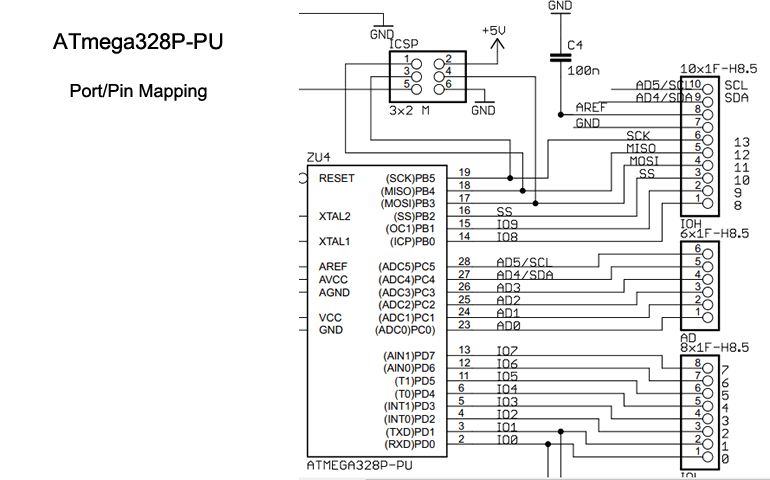
- Insert a bicolor LED into the UNO pins 12 and 13, and any LED in pins 10 and 11.
- What port of the ATmega328P are these pins associated with? What port BITS are these pins mapped to?
- Within your setup() function, use the relevant GPIO register name to declare ALL of port B's (available) digital pins for output (in lieu of the high-level pinMode() function).
- (Register-Level Blink Sketch) Within your loop() function, employ precise bit-level IO register statements (in lieu of digitalWrite() statements) targeted at pins 12 and 13, add code to have pin 13 provide the anode signal and pin 12, the cathode signal. Upload the sketch and confirm.
- Add code to provide a 1s delay, before employing precision register-level statements to pins 12 and 13 to reverse the anode and cathode. Add another 1s delay before uploading and confirming.
- Can the alternation described in tasks 6 and 7 be done with a single assignment statement and delay?
Statements for YOUR Consideration
 What do each of the following GPIO Register-Level assignment statements accomplish? (the last two are beauties as they have particular meaning for us) Attention 11s and 12s: Be the FIRST to correctly identify what (recent) special purpose BOTH of these hold for ACES, in SINGLE email to the ICS3UForum under the Subject Line: Bit Banging and you will win a LARGE bag of Bits & Bites ->>>>
- DDRD = 0xF0; //insert comment here
- PORTB |= 1; //insert comment here
- PORTC = ~PORTC; //insert comment here
- PORTD &= 0x0F; //insert comment here
- PORTD |= 1; //insert comment here
- PORTB |= 1<<PB5 | 1<<PB2; //insert comment here
- PORTD ^= PORTD; //insert comment here
- PIND |= 1<<PD2; //insert comment here
- response = PIND; //insert comment here
Further Topics...
- Defining literals
- Displaying numeric literals
- Explore binary-related methods of the Integer Class
- Counting Bits (Parity)
- Bit Shifting: <<, >>
- Masking Bits: Odd/Even; Upper- or Lowercase
- Negative Numbers (2's Complement Strategy)
- Arithmetic. Adders (Half Adders and Full Adders)